JAJSER9C December   2017  – March 2023 LMZM23601

PRODUCTION DATA  

  1. 特長
  2. アプリケーション
  3. 概要
  4. Revision History
    1.     Device Comparison
  5. Pin Configuration and Functions
  6. Specifications
    1. 6.1 Absolute Maximum Ratings
    2. 6.2 ESD Ratings
    3. 6.3 Recommended Operating Conditions
    4. 6.4 Thermal Information
    5. 6.5 Electrical Characteristics
    6. 6.6 System Characteristics
    7. 6.7 Typical Characteristics
  7. Detailed Description
    1. 7.1 Overview
    2. 7.2 Functional Block Diagram
    3. 7.3 Feature Description
      1. 7.3.1 Control Scheme
      2. 7.3.2 Soft-Start Function
      3. 7.3.3 Enable and External UVLO Function
      4. 7.3.4 Current Limit
      5. 7.3.5 Hiccup Mode
      6. 7.3.6 Power Good (PGOOD) Function
      7. 7.3.7 MODE/SYNC Function
        1. 7.3.7.1 Forced PWM Mode
        2. 7.3.7.2 Auto PFM Mode
        3. 7.3.7.3 Dropout Mode
        4. 7.3.7.4 SYNC Operation
      8. 7.3.8 Thermal Protection
    4. 7.4 Device Functional Modes
      1. 7.4.1 Shutdown
      2. 7.4.2 FPWM Operation
      3. 7.4.3 Auto PFM Mode Operation
  8. Application and Implementation
    1. 8.1 Application Information
    2. 8.2 Typical Applications
      1. 8.2.1 Design Requirements
        1. 8.2.1.1 Maximum Input Voltage for VOUT < 2.5 V
      2. 8.2.2 Detailed Design Procedure
        1. 8.2.2.1 Custom Design With WEBENCH® Tools
        2. 8.2.2.2 Input Capacitor Selection
        3. 8.2.2.3 Output Capacitor Selection
        4. 8.2.2.4 Feedback Voltage Divider for Adjustable Output Voltage Versions
        5. 8.2.2.5 RPU - PGOOD Pullup Resistor
        6. 8.2.2.6 VIN Divider and Enable
      3. 8.2.3 Application Curves
        1. 8.2.3.1 VOUT = 5 V
        2. 8.2.3.2 VOUT = 3.3 V
        3. 8.2.3.3 VOUT = 12 V
        4. 8.2.3.4 VOUT = 15 V
        5. 8.2.3.5 VOUT = 2.5 V
        6. 8.2.3.6 VOUT = 1.2 V and VOUT = 1.8 V
        7. 8.2.3.7 VOUT = 5 V and 3.3 V Fixed Output Options
    3. 8.3 Best Design Practices
    4. 8.4 Power Supply Recommendations
      1. 8.4.1 Supply Voltage Range
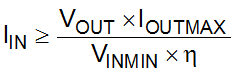
      2. 8.4.2 Supply Current Capability
      3. 8.4.3 Supply Input Connections
        1. 8.4.3.1 Voltage Drops
        2. 8.4.3.2 Stability
    5. 8.5 Layout
      1. 8.5.1 Layout Guidelines
        1. 8.5.1.1 Thermal Design
      2. 8.5.2 Layout Examples
  9. Device and Documentation Support
    1. 9.1 Device Support
      1. 9.1.1 サード・パーティ製品に関する免責事項
      2. 9.1.2 Development Support
        1. 9.1.2.1 Custom Design With WEBENCH® Tools
    2. 9.2 Documentation Support
      1. 9.2.1 Related Documentation
    3. 9.3 ドキュメントの更新通知を受け取る方法
    4. 9.4 サポート・リソース
    5. 9.5 Trademarks
    6. 9.6 静電気放電に関する注意事項
    7. 9.7 用語集
  10. 10Mechanical, Packaging, and Orderable Information
    1. 10.1 Tape and Reel Information

パッケージ・オプション

デバイスごとのパッケージ図は、PDF版データシートをご参照ください。

メカニカル・データ(パッケージ|ピン)
  • SIL|10
サーマルパッド・メカニカル・データ
発注情報

Supply Current Capability

The input supply must be able to supply the required input current to the LMZM23601 converter. The required input current depends on the application's minimum input voltage, the required maximum output current, the output voltage, and the converter efficiency η for this condition.

Equation 4. GUID-E4841F63-7241-442E-B828-488C0FE453D3-low.gif

As an example, assuming that the adjustable output voltage version of the LMZM23601 is used for a 5-V, 1-A output converter design with 12-V minimum input voltage. The conversion efficiency for this condition is about 85%. The required input current from the supply is 0.49 A, so TI recommends an input power supply with ≥ 0.5 A current capability.