JAJSER9C December   2017  – March 2023 LMZM23601

PRODUCTION DATA  

  1. 特長
  2. アプリケーション
  3. 概要
  4. Revision History
    1.     Device Comparison
  5. Pin Configuration and Functions
  6. Specifications
    1. 6.1 Absolute Maximum Ratings
    2. 6.2 ESD Ratings
    3. 6.3 Recommended Operating Conditions
    4. 6.4 Thermal Information
    5. 6.5 Electrical Characteristics
    6. 6.6 System Characteristics
    7. 6.7 Typical Characteristics
  7. Detailed Description
    1. 7.1 Overview
    2. 7.2 Functional Block Diagram
    3. 7.3 Feature Description
      1. 7.3.1 Control Scheme
      2. 7.3.2 Soft-Start Function
      3. 7.3.3 Enable and External UVLO Function
      4. 7.3.4 Current Limit
      5. 7.3.5 Hiccup Mode
      6. 7.3.6 Power Good (PGOOD) Function
      7. 7.3.7 MODE/SYNC Function
        1. 7.3.7.1 Forced PWM Mode
        2. 7.3.7.2 Auto PFM Mode
        3. 7.3.7.3 Dropout Mode
        4. 7.3.7.4 SYNC Operation
      8. 7.3.8 Thermal Protection
    4. 7.4 Device Functional Modes
      1. 7.4.1 Shutdown
      2. 7.4.2 FPWM Operation
      3. 7.4.3 Auto PFM Mode Operation
  8. Application and Implementation
    1. 8.1 Application Information
    2. 8.2 Typical Applications
      1. 8.2.1 Design Requirements
        1. 8.2.1.1 Maximum Input Voltage for VOUT < 2.5 V
      2. 8.2.2 Detailed Design Procedure
        1. 8.2.2.1 Custom Design With WEBENCH® Tools
        2. 8.2.2.2 Input Capacitor Selection
        3. 8.2.2.3 Output Capacitor Selection
        4. 8.2.2.4 Feedback Voltage Divider for Adjustable Output Voltage Versions
        5. 8.2.2.5 RPU - PGOOD Pullup Resistor
        6. 8.2.2.6 VIN Divider and Enable
      3. 8.2.3 Application Curves
        1. 8.2.3.1 VOUT = 5 V
        2. 8.2.3.2 VOUT = 3.3 V
        3. 8.2.3.3 VOUT = 12 V
        4. 8.2.3.4 VOUT = 15 V
        5. 8.2.3.5 VOUT = 2.5 V
        6. 8.2.3.6 VOUT = 1.2 V and VOUT = 1.8 V
        7. 8.2.3.7 VOUT = 5 V and 3.3 V Fixed Output Options
    3. 8.3 Best Design Practices
    4. 8.4 Power Supply Recommendations
      1. 8.4.1 Supply Voltage Range
      2. 8.4.2 Supply Current Capability
      3. 8.4.3 Supply Input Connections
        1. 8.4.3.1 Voltage Drops
        2. 8.4.3.2 Stability
    5. 8.5 Layout
      1. 8.5.1 Layout Guidelines
        1. 8.5.1.1 Thermal Design
      2. 8.5.2 Layout Examples
  9. Device and Documentation Support
    1. 9.1 Device Support
      1. 9.1.1 サード・パーティ製品に関する免責事項
      2. 9.1.2 Development Support
        1. 9.1.2.1 Custom Design With WEBENCH® Tools
    2. 9.2 Documentation Support
      1. 9.2.1 Related Documentation
    3. 9.3 ドキュメントの更新通知を受け取る方法
    4. 9.4 サポート・リソース
    5. 9.5 Trademarks
    6. 9.6 静電気放電に関する注意事項
    7. 9.7 用語集
  10. 10Mechanical, Packaging, and Orderable Information
    1. 10.1 Tape and Reel Information

パッケージ・オプション

デバイスごとのパッケージ図は、PDF版データシートをご参照ください。

メカニカル・データ(パッケージ|ピン)
  • SIL|10
サーマルパッド・メカニカル・データ
発注情報

Feedback Voltage Divider for Adjustable Output Voltage Versions

GUID-5A7EE108-691C-458A-B348-073AE5BE42FE-low.gifFigure 8-4 Adjustable 1.2-V to 15-V Output Typical Application Circuit

The adjustable version of the LMZM23601 regulates the output voltage such that the FB node voltage is equal to the internal VREF voltage of 1 V. The output voltage is then set by a feedback voltage divider formed by two external resistors, RFBT and RFBB.

Equation 1. GUID-5459B3C6-12C7-43C5-AE72-11DD6302E36B-low.gif

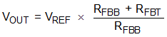
The range of adjustable output voltage is 1.2 V to 15 V.

Choose a value for RFBT in the kΩ range, and calculate the bottom resistor RFBB using Equation 2:

Equation 2. GUID-F5D9F705-9061-4E1F-A3F5-CC37900DB4C5-low.gif

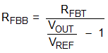
For VOUT < 3.0 V, TI recommends to allow 20 µA of static load current on the output. This can be achieved by limiting the maximum resistance of the feedback divider. For example, for VOUT = 2 V, the maximum total feedback resistance (RFBB+ RFBT) must be 100 kΩ or less.

For this design example the output voltage is set to 5 V. The fixed 5-V output voltage option of the LMZM23601 can be used without any feedback resistors. If the adjustable output option is used for this design condition, the top feedback resistor RFBT can be set to 102 kΩ. The RFBB value results in 25.5 kΩ.