JAJS700Q November 1999 – October 2016 LP2985LV-N
PRODUCTION DATA.
- 1 特長
- 2 アプリケーション
- 3 概要
- 4 改訂履歴
- 5 Pin Configuration and Functions
- 6 Specifications
- 7 Detailed Description
-
8 Application and Implementation
- 8.1 Application Information
- 8.2 Typical Application
- 9 Power Supply Recommendations
- 10Layout
- 11デバイスおよびドキュメントのサポート
- 12メカニカル、パッケージ、および注文情報
6 Specifications
6.1 Absolute Maximum Ratings
over operating free-air temperature range (unless otherwise noted)(1)(2)| MIN | MAX | UNIT | ||
|---|---|---|---|---|
| Input supply voltage | –0.3 | 16 | V | |
| Shutdown input voltage | –0.3 | 16 | V | |
| Power dissipation(3) | Internally Limited | |||
| Output voltage(4) | –0.3 | 9 | V | |
| IOUT | Short-circuit protected | |||
| Input-output voltage(5) | –0.3 | 16 | V | |
| Storage temperature, Tstg | –65 | 150 | °C | |
(1) Stresses beyond those listed under Absolute Maximum Ratings may cause permanent damage to the device. These are stress ratings only, which do not imply functional operation of the device at these or any other conditions beyond those indicated under Recommended Operating Conditions. Exposure to absolute-maximum-rated conditions for extended periods may affect device reliability.
(2) If Military/Aerospace specified devices are required, contact the Texas Instruments Sales Office/ Distributors for availability and specifications.
(3) The maximum allowable power dissipation is a function of the maximum junction temperature, TJ_MAX, the junction-to-ambient thermal resistance, RθJA, and the ambient temperature, TA. The maximum allowable power dissipation at any ambient temperature is calculated using:

Where the value of RθJA for the SOT-23 package is 175.7°C/W in a typical PC board mounting or 178.8°C/W for YPB-type DSBGA package.
Exceeding the maximum allowable dissipation causes excessive die temperature, and the regulator goes into thermal shutdown.

Where the value of RθJA for the SOT-23 package is 175.7°C/W in a typical PC board mounting or 178.8°C/W for YPB-type DSBGA package.
Exceeding the maximum allowable dissipation causes excessive die temperature, and the regulator goes into thermal shutdown.
(4) If used in a dual-supply system where the regulator load is returned to a negative supply, the LP2985LV-N output must be diode-clamped to GND.
(5) The output PNP structure contains a diode between the IN to OUT pins that is normally reverse-biased. Reversing the polarity from IN to OUT turns on this diode.
6.2 ESD Ratings
| VALUE | UNIT | ||||
|---|---|---|---|---|---|
| V(ESD) | Electrostatic discharge | Human-body model (HBM), per ANSI/ESDA/JEDEC JS-001(1) | Pins 3 and 4 (SOT-23) Pins A3 and B2 (DSBGA) |
±1000 | V |
| Pins 1, 2, and 5 (SOT-23) Pins A1, C1, and C3 (DSBGA) |
±2000 | ||||
(1) JEDEC document JEP155 states that 500-V HBM allows safe manufacturing with a standard ESD control process.
6.3 Recommended Operating Conditions
over operating free-air temperature range (unless otherwise noted)| MIN | MAX | UNIT | |||
|---|---|---|---|---|---|
| VIN | Supply input voltage | 2.2(1) | 16 | V | |
| VON/OFF | ON/OFF input voltage | 0 | VIN | V | |
| IOUT | Output current | 150 | mA | ||
| TJ | Operating junction temperature | –40 | 125 | °C | |
(1) Recommended minimum VIN is the greater of 2.2 V or VOUT(MAX) + rated dropout voltage (maximum) for operating load current.
6.4 Thermal Information
| THERMAL METRIC(1) | LP2985LV-N | UNIT | ||
|---|---|---|---|---|
| SOT-23 (DBV) | DSBGA (YPB) | |||
| 5 PINS | ||||
| RθJA(2) | Junction-to-ambient thermal resistance | 175.7 | 178.8 | °C/W |
| RθJC(top) | Junction-to-case (top) thermal resistance | 78 | 2.1 | °C/W |
| RθJB | Junction-to-board thermal resistance | 30.8 | 146.3 | °C/W |
| ψJT | Junction-to-top characterization parameter | 2.8 | 1.9 | °C/W |
| ψJB | Junction-to-board characterization parameter | 30.3 | 146.3 | °C/W |
(1) For more information about traditional and new thermal metrics, see the Semiconductor and IC Package Thermal Metrics application report.
(2) Thermal resistance value RθJA is based on the EIA/JEDEC High-K printed circuit board defined by: JESD51-7 - High Effective Thermal Conductivity Test Board for Leaded Surface Mount Packages.
6.5 Electrical Characteristics
Unless otherwise specified: VIN = VO(NOM) + 1 V, IL = 1 mA, CIN = 1 µF, COUT = 4.7 µF, VON/OFF = 2 V, TJ = 25°C.(1)| PARAMETER | TEST CONDITIONS | LP2985AI-XX(2) | LP2985I-XX(2) | UNIT | |||||
|---|---|---|---|---|---|---|---|---|---|
| MIN | TYP | MAX | MIN | TYP | MAX | ||||
| ΔVO | Output voltage tolerance | IL = 1 mA | −1 | 1 | −1.5 | 1.5 | %VNOM | ||
| 1 mA < IL < 50 mA | −1.5 | 1.5 | −2.5 | 2.5 | |||||
| 1 mA < IL < 50 mA –40°C ≤ TJ ≤ 125°C |
−2.5 | 2.5 | −3.5 | 3.5 | |||||
| 1 mA < IL < 150 mA | −2.5 | 2.5 | −3 | 3 | |||||
| 1 mA < IL < 150 mA –40°C ≤ TJ ≤ 125°C |
−3.5 | 3.5 | −4 | 4 | |||||
| ΔVO/ΔVIN | Output voltage line regulation | VO(NOM) + 1 V ≤ VIN ≤ 16 V | 0.007 | 0.014 | 0.007 | 0.014 | %/V | ||
| VO(NOM) + 1 V ≤ VIN ≤ 16 V –40°C ≤ TJ ≤ 125°C |
0.032 | 0.032 | |||||||
| VIN(MIN) | Minimum input voltage required to maintain output regulation(3) | 2.05 | 2.05 | V | |||||
| –40°C ≤ TJ ≤ 125°C | 2.2 | 2.2 | |||||||
| VIN – VOUT | Dropout voltage(3) | IL = 50 mA | 120 | 150 | 120 | 150 | mV | ||
| IL = 50 mA, –40°C ≤ TJ ≤ 125°C | 250 | 250 | |||||||
| IL = 150 mA | 280 | 350 | 280 | 350 | |||||
| IL = 150 mA, –40°C ≤ TJ ≤ 125°C | 600 | 600 | |||||||
| IGND | Ground pin current | IL = 0 mA | 65 | 95 | 65 | 95 | μA | ||
| IL = 0 mA, –40°C ≤ TJ ≤ 125°C | 125 | 125 | |||||||
| IL = 1 mA | 75 | 110 | 75 | 110 | |||||
| IL = 1 mA, –40°C ≤ TJ ≤ 125°C | 170 | 170 | |||||||
| IL = 10 mA | 120 | 220 | 120 | 220 | |||||
| IL = 10 mA, –40°C ≤ TJ ≤ 125°C | 400 | 400 | |||||||
| IL = 50 mA | 300 | 500 | 300 | 500 | |||||
| IL = 50 mA, –40°C ≤ TJ ≤ 125°C | 900 | 900 | |||||||
| IL = 150 mA | 825 | 1200 | 825 | 1200 | |||||
| IL = 150 mA, –40°C ≤ TJ ≤ 125°C | 2000 | 2000 | |||||||
| VON/OFF < 0.3 V | 0.01 | 0.8 | 0.01 | 0.8 | |||||
| VON/OFF < 0.15 V –40°C ≤ TJ ≤ 125°C |
0.05 | 2 | 0.05 | 2 | |||||
| VON/OFF | ON/OFF input voltage(4) | High = O/P ON | 1.4 | 1.4 | V | ||||
| High = O/P ON –40°C ≤ TJ ≤ 125°C |
1.6 | 1.6 | |||||||
| Low = O/P OFF | 0.55 | 0.55 | |||||||
| Low = O/P OFF –40°C ≤ TJ ≤ 125°C |
0.15 | 0.15 | |||||||
| ION/OFF | ON/OFF input current | VON/OFF = 0 V | 0.01 | 0.01 | μA | ||||
| VON/OFF = 0 V –40°C ≤ TJ ≤ 125°C |
–2 | –2 | |||||||
| VON/OFF = 5 V | 5 | 5 | |||||||
| VON/OFF = 5 V –40°C ≤ TJ ≤ 125°C |
15 | 15 | |||||||
| IO(PK) | Peak output current | VOUT ≥ VO(NOM) − 5% | 350 | 350 | mA | ||||
| en | Output noise voltage | BW = 300 Hz to 50 kHz COUT = 10 μF CBYPASS = 10 nF, VOUT = 1.8 V |
30 | 30 | μV(RMS) | ||||
| ΔVO/ΔVIN | Ripple rejection | ƒ = 1 kHz, COUT = 10 μF CBYPASS = 10 nF |
45 | 45 | dB | ||||
| IO(SC) | Short-circuit current | RL = 0 Ω (steady state)(5) | 400 | 400 | mA | ||||
(1) Exposing the DSBGA device to direct sunlight causes misoperation. See Layout for additional information.
(2) Limits are 100% production tested at 25°C. Limits over the operating temperature range are ensured through correlation using statistical quality control (SQC) methods. The limits are used to calculate average outgoing quality level (AOQL).
(3) VIN must be the greater of 2.2 V or VOUT(NOM) + dropout voltage to maintain output regulation. Dropout voltage is defined as the input to output differential at which the output voltage drops 2% below the value measured with a 1-V differential.
(4) The ON/OFF inputs must be properly driven to prevent misoperation. For details, see Operation With ON/OFF Control.
(5) The LP2985LV-N has foldback current limiting, which allows a high peak current when VOUT > 0.5 V and then reduces the maximum output current as VOUT is forced to ground (see related curve(s) in Typical Characteristics).
6.6 Typical Characteristics
Unless otherwise specified: CIN = 1 µF, COUT = 4. 7µF, VIN = VOUT(NOM) + 1, VOUT = 1.8 V, TA = 25°C, ON/OFF pin is tied to VIN.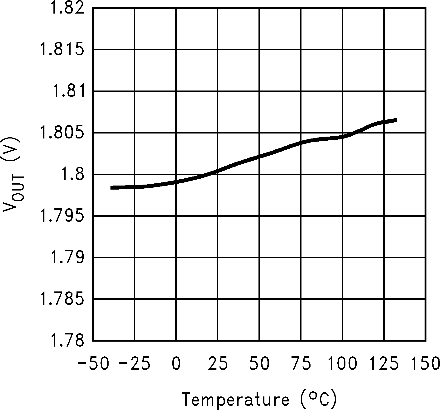 Figure 1. VOUT vs Temperature
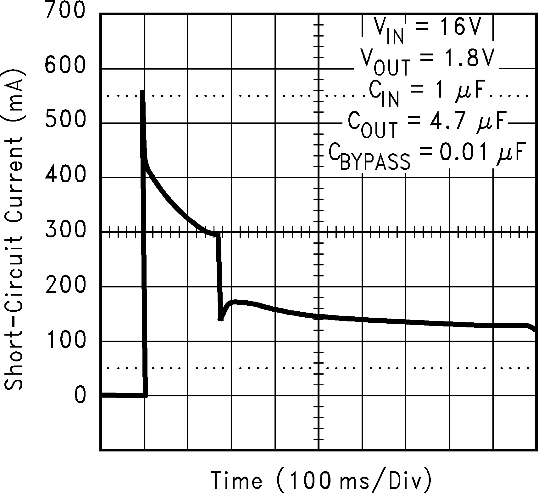
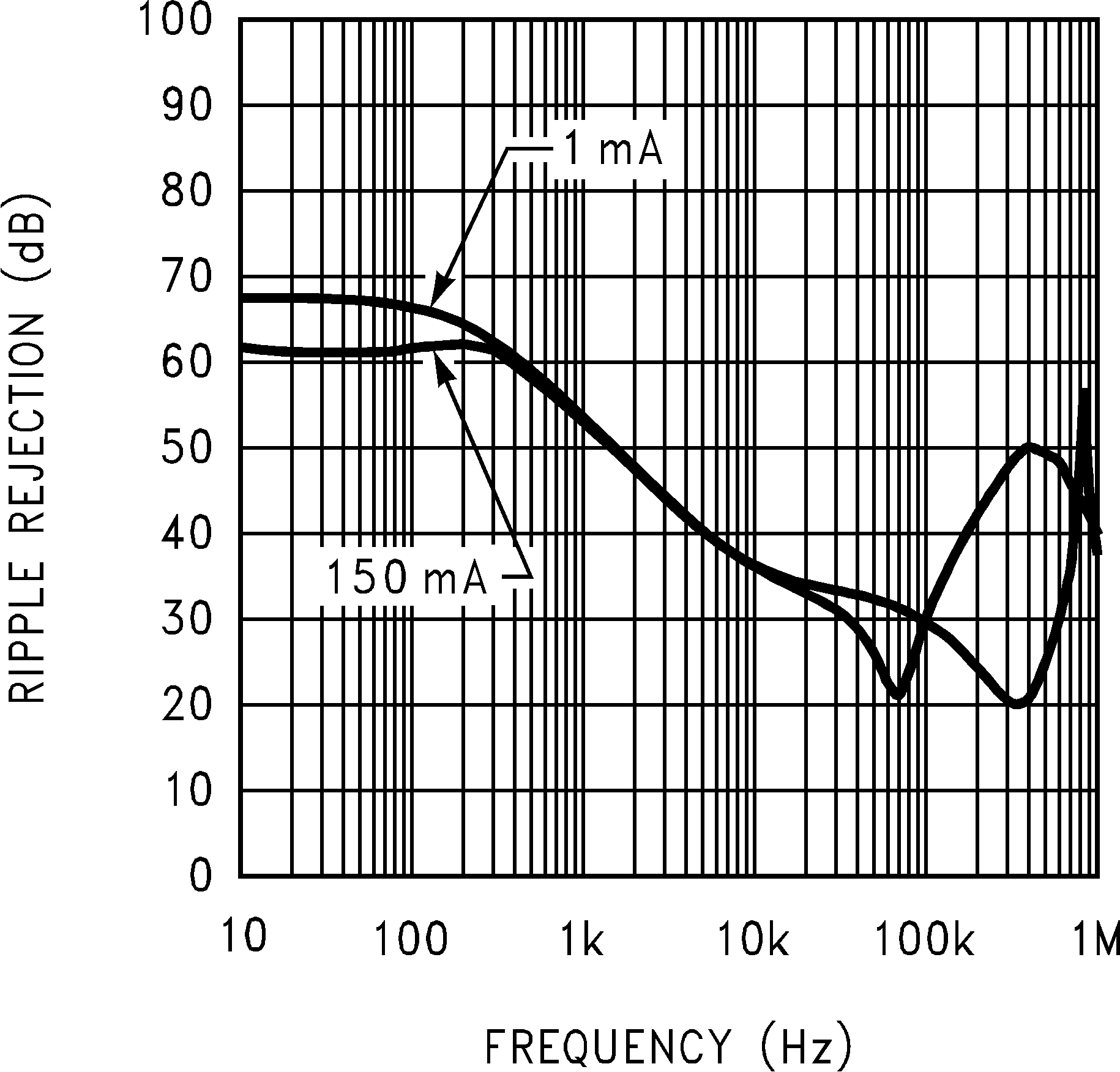
| COUT = 4.7 µF | Bypass = 10 nF |
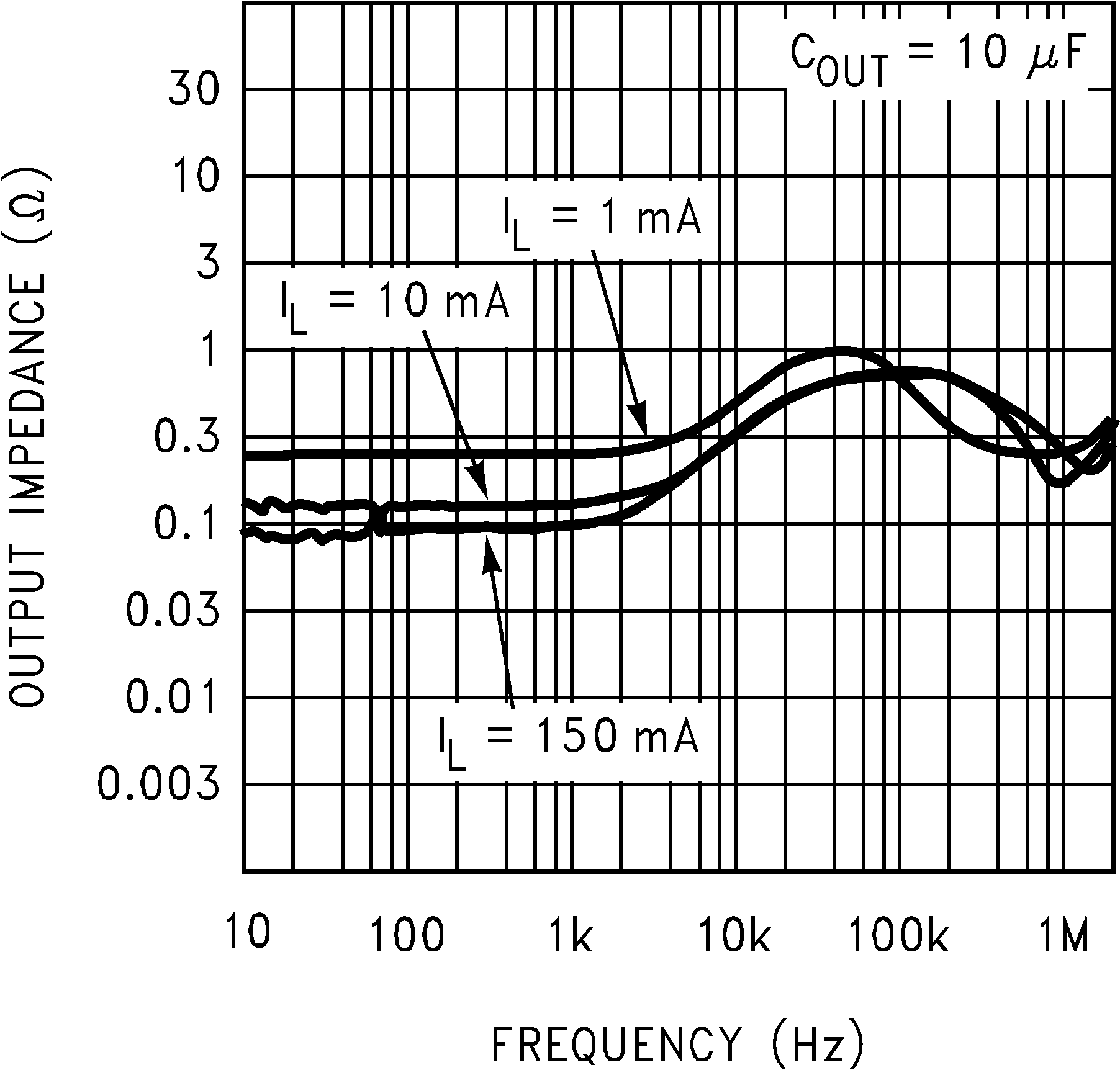 Figure 7. Output Impedance vs Frequency
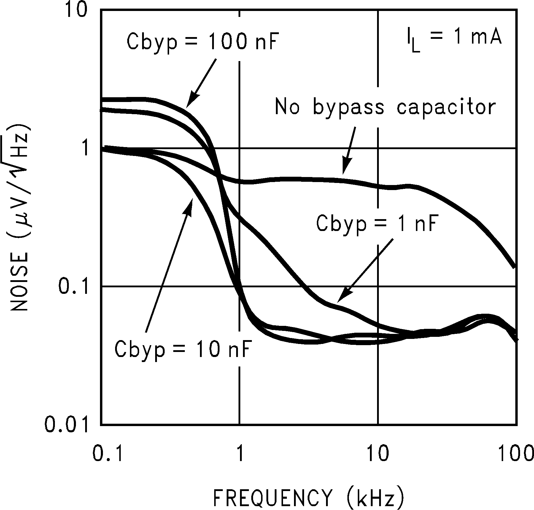 Figure 9. Noise Density
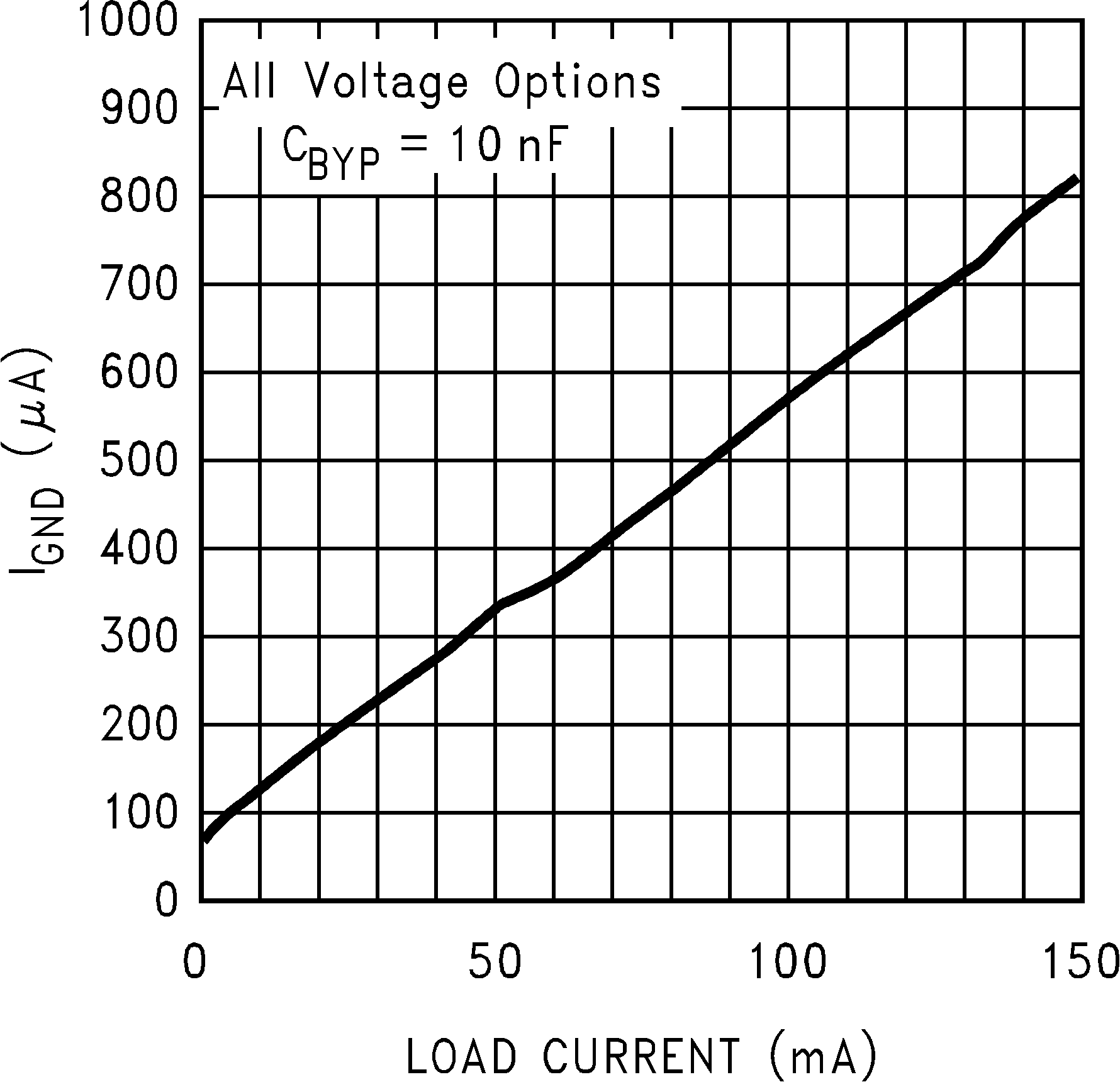 Figure 11. Ground Pin vs Load Current
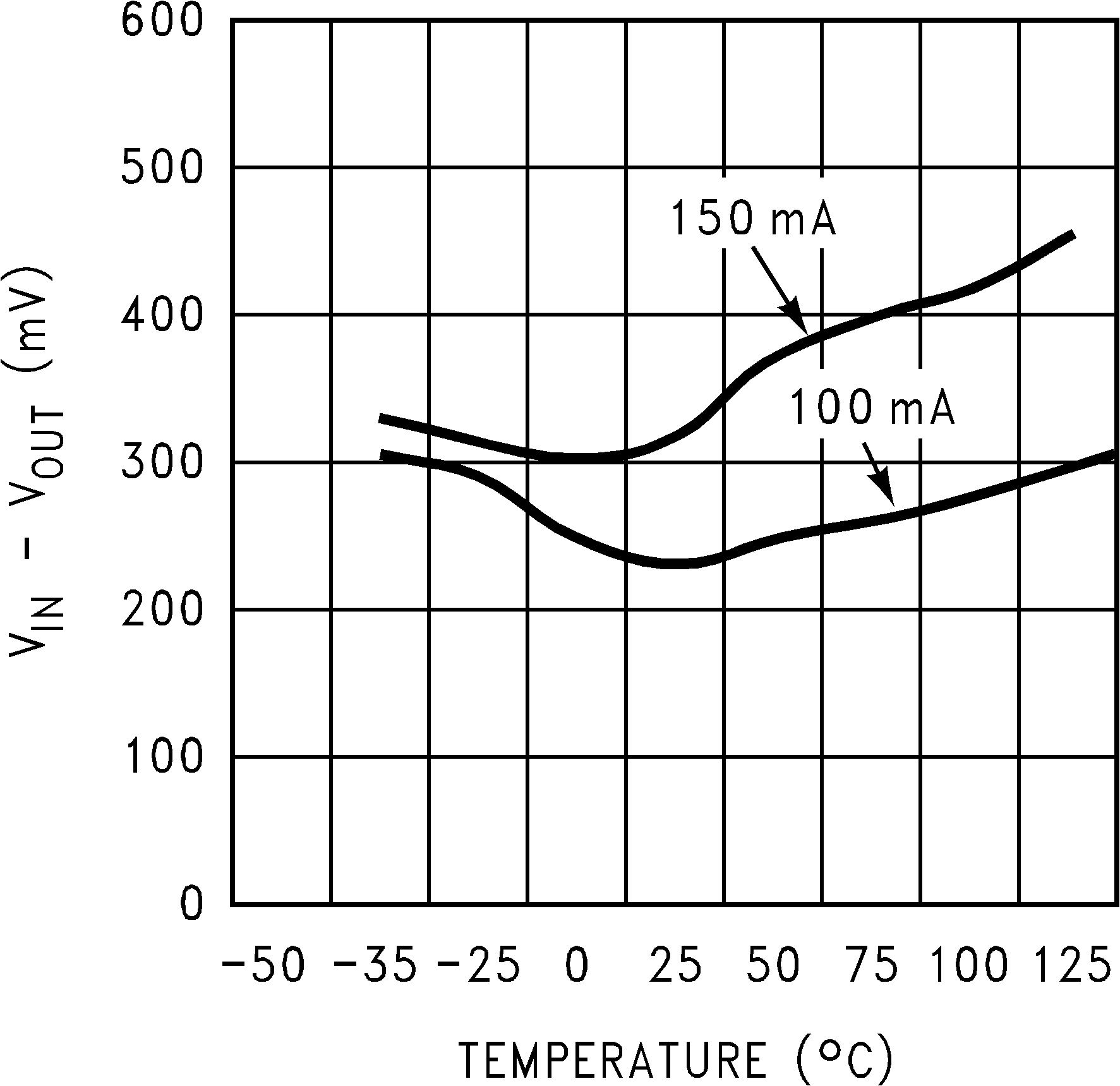 Figure 13. Minimum Input Voltage vs Temperature
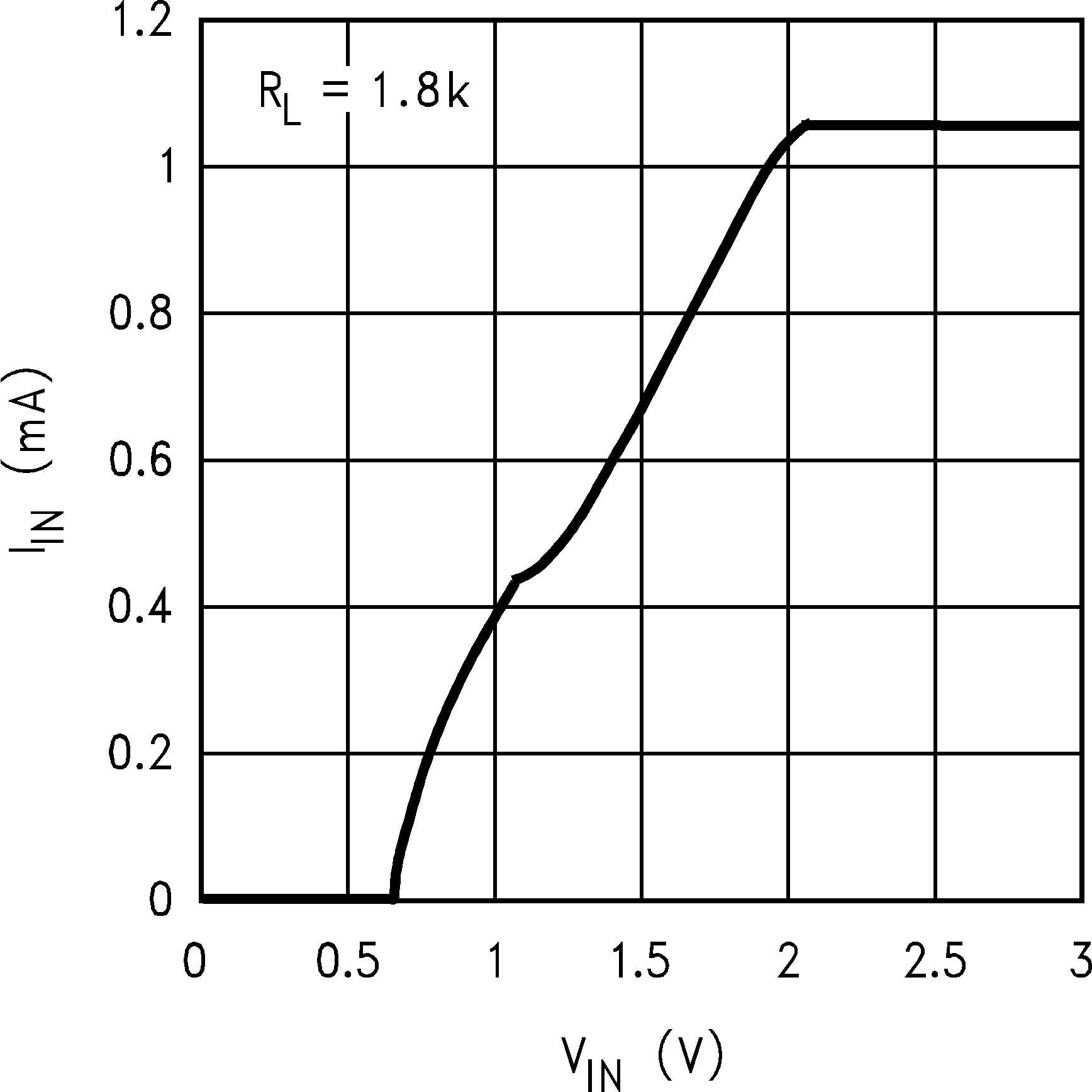 Figure 15. Input Current vs VIN
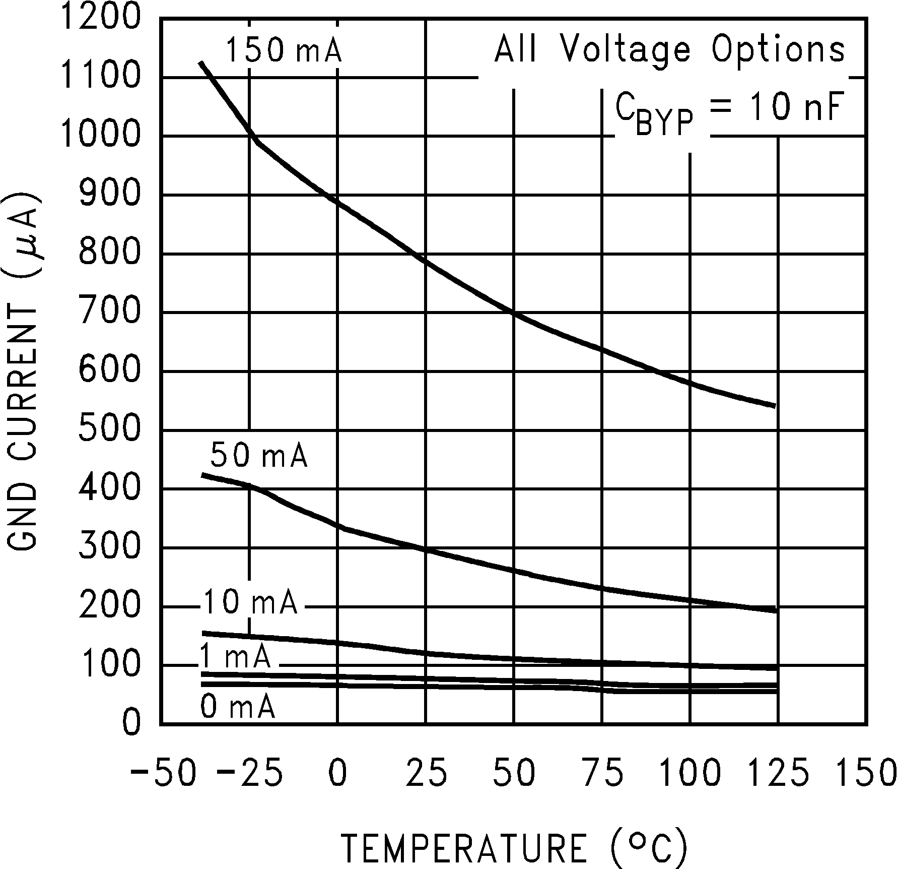 Figure 17. Ground Pin Current vs Temperature
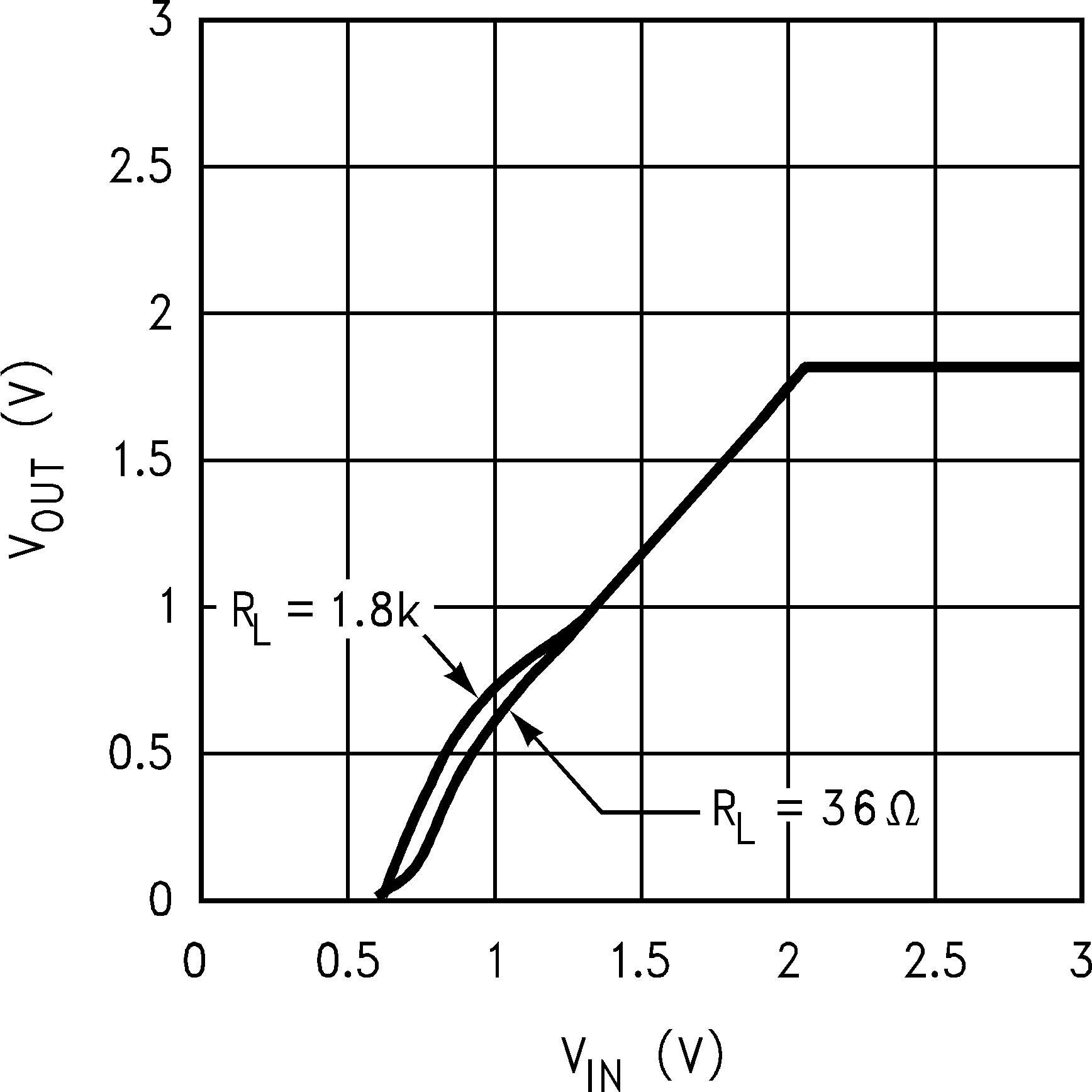 Figure 19. Output Characteristics
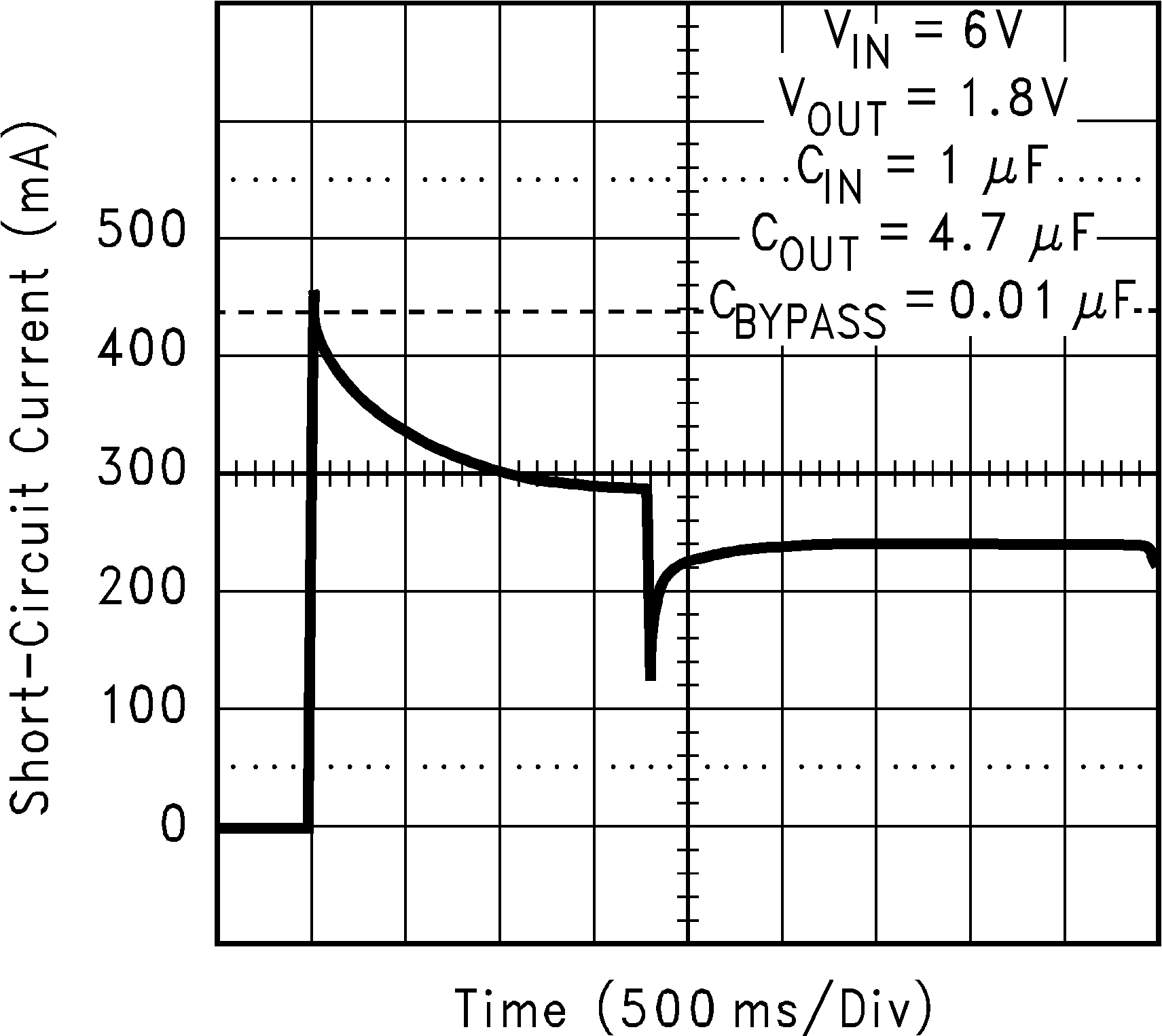
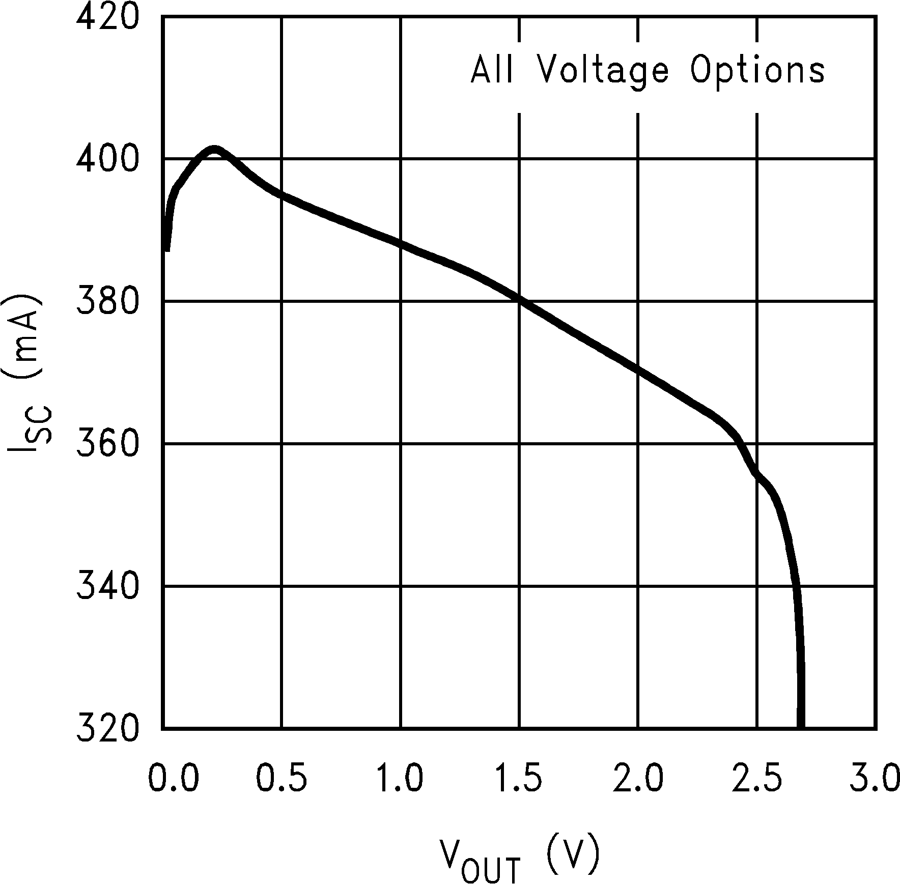 Figure 4. Short-Circuit Current vs Output Voltage
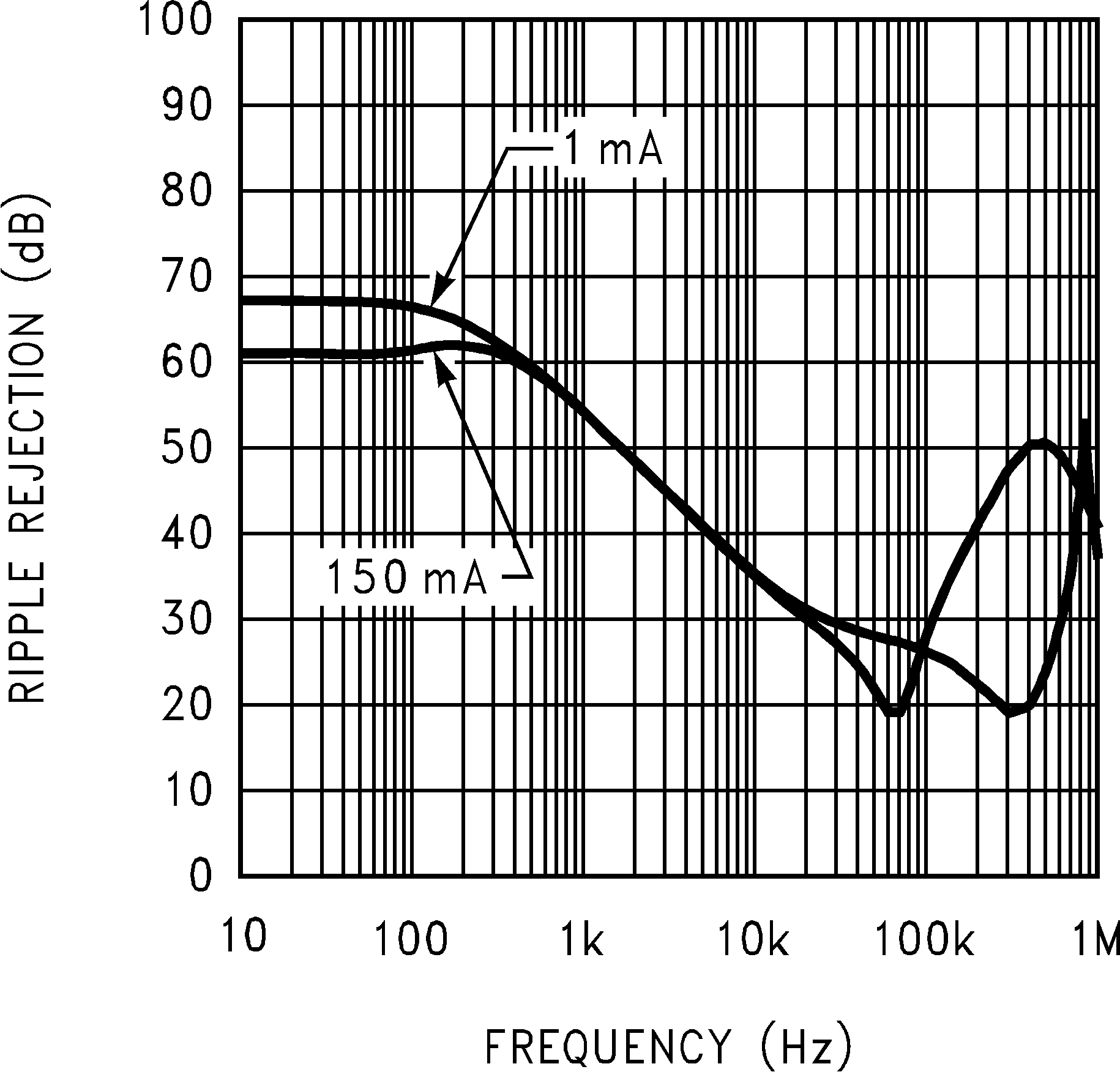
| COUT = 4.7 µF | No Bypass |
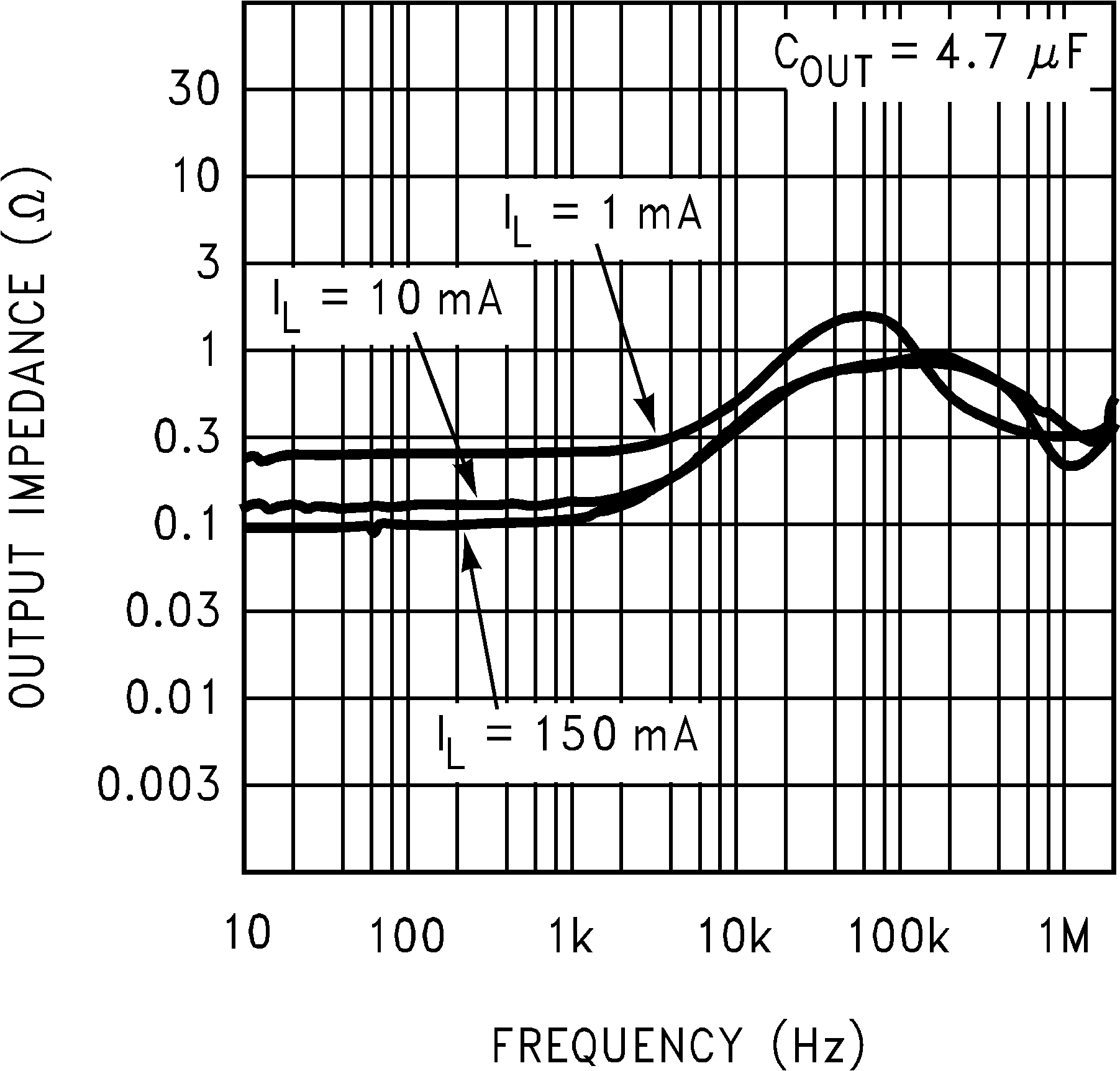 Figure 8. Output Impedance vs Frequency
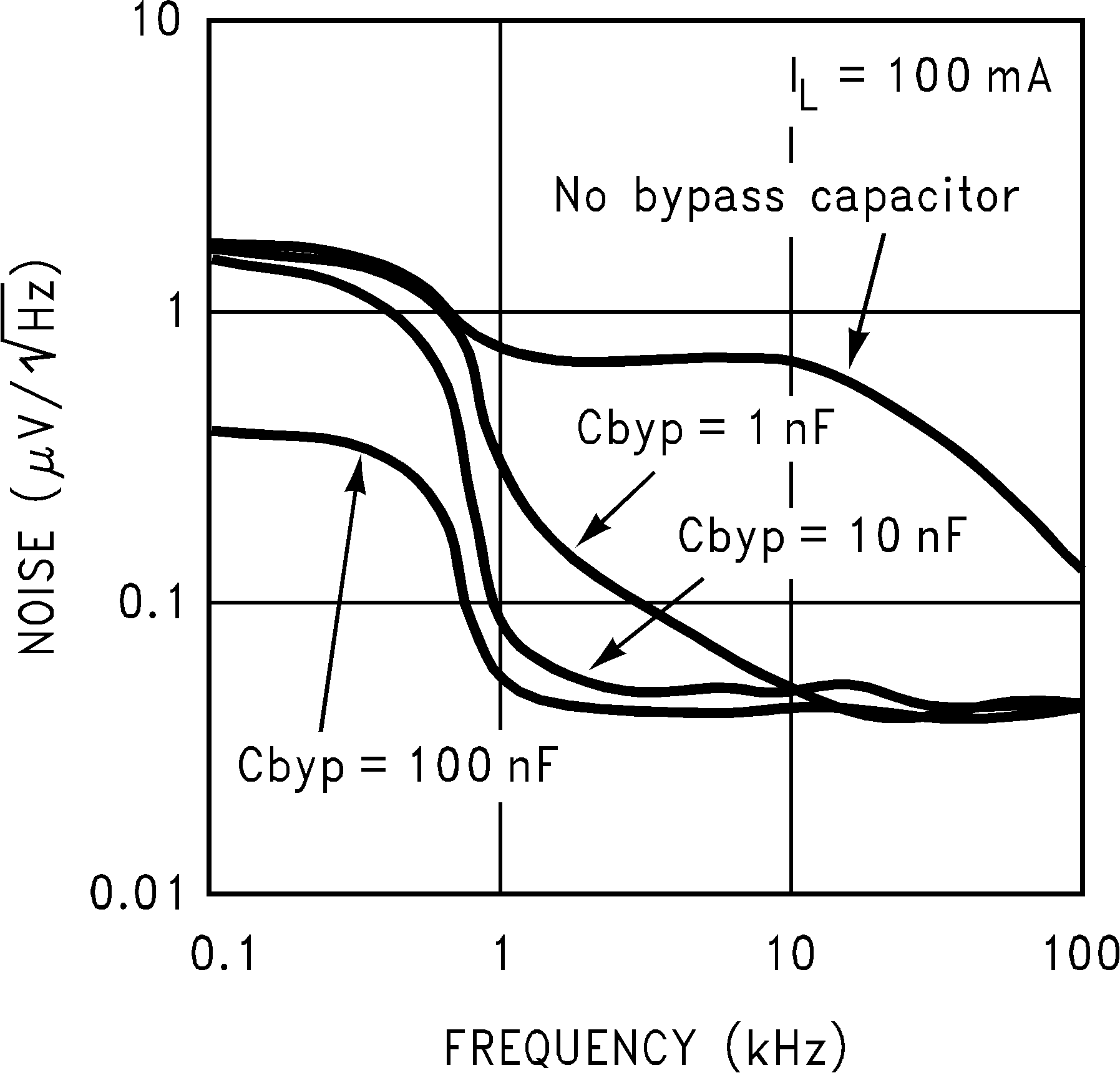 Figure 10. Noise Density
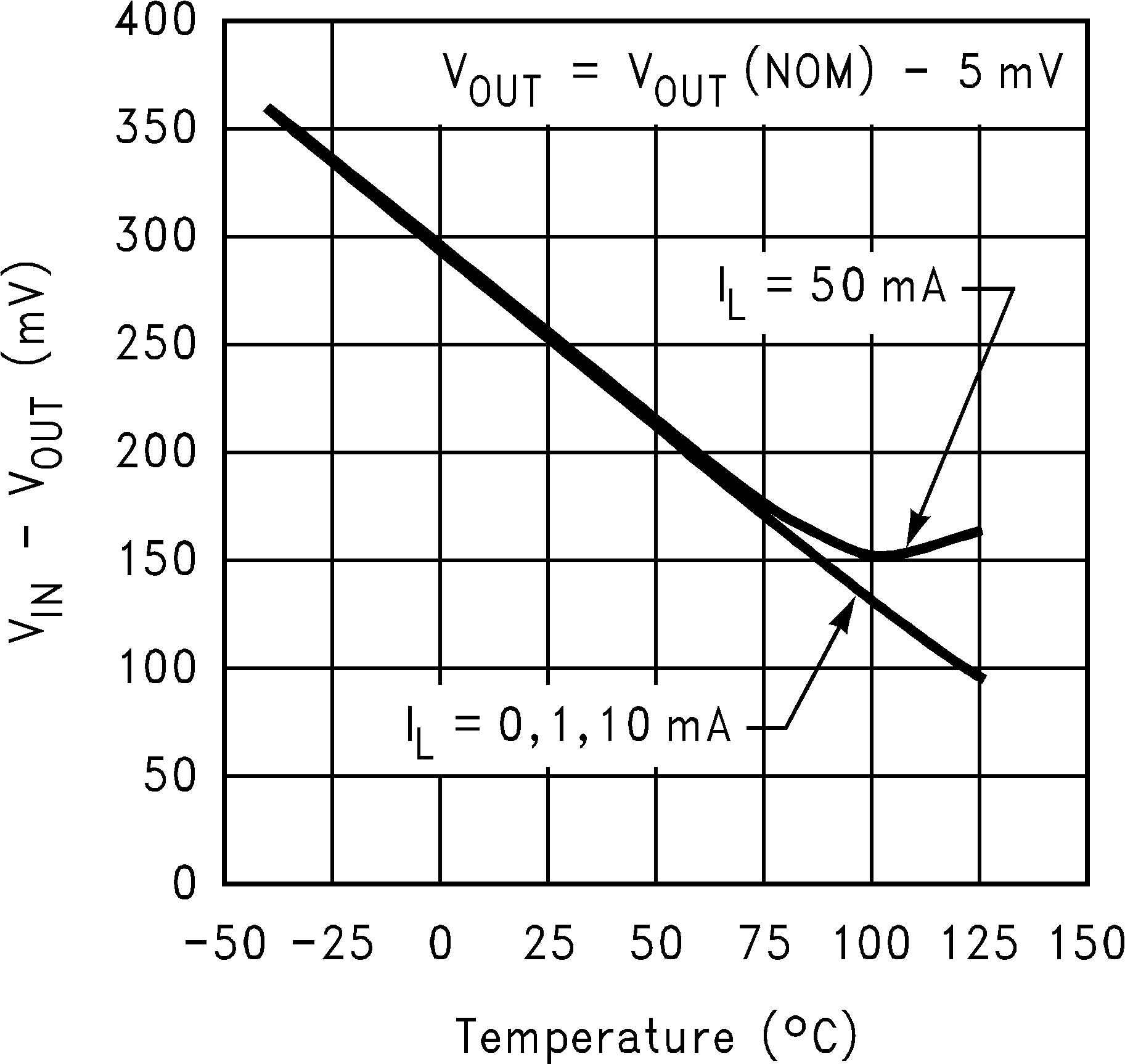 Figure 12. Minimum Input Voltage vs Temperature
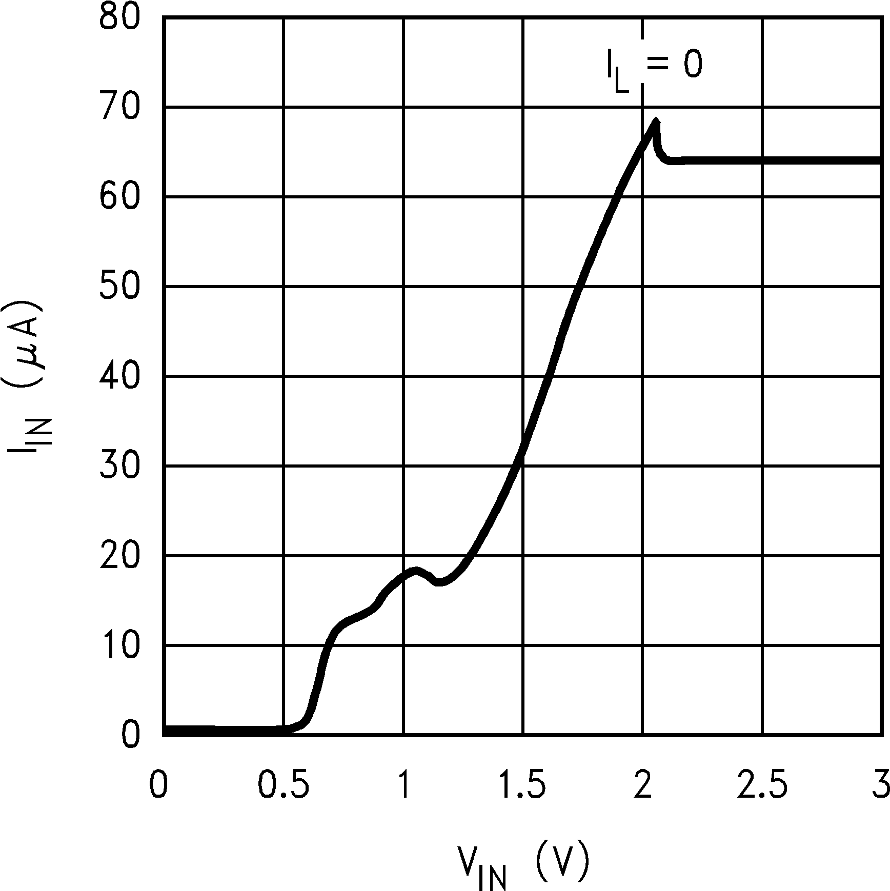 Figure 14. Input Current vs VIN
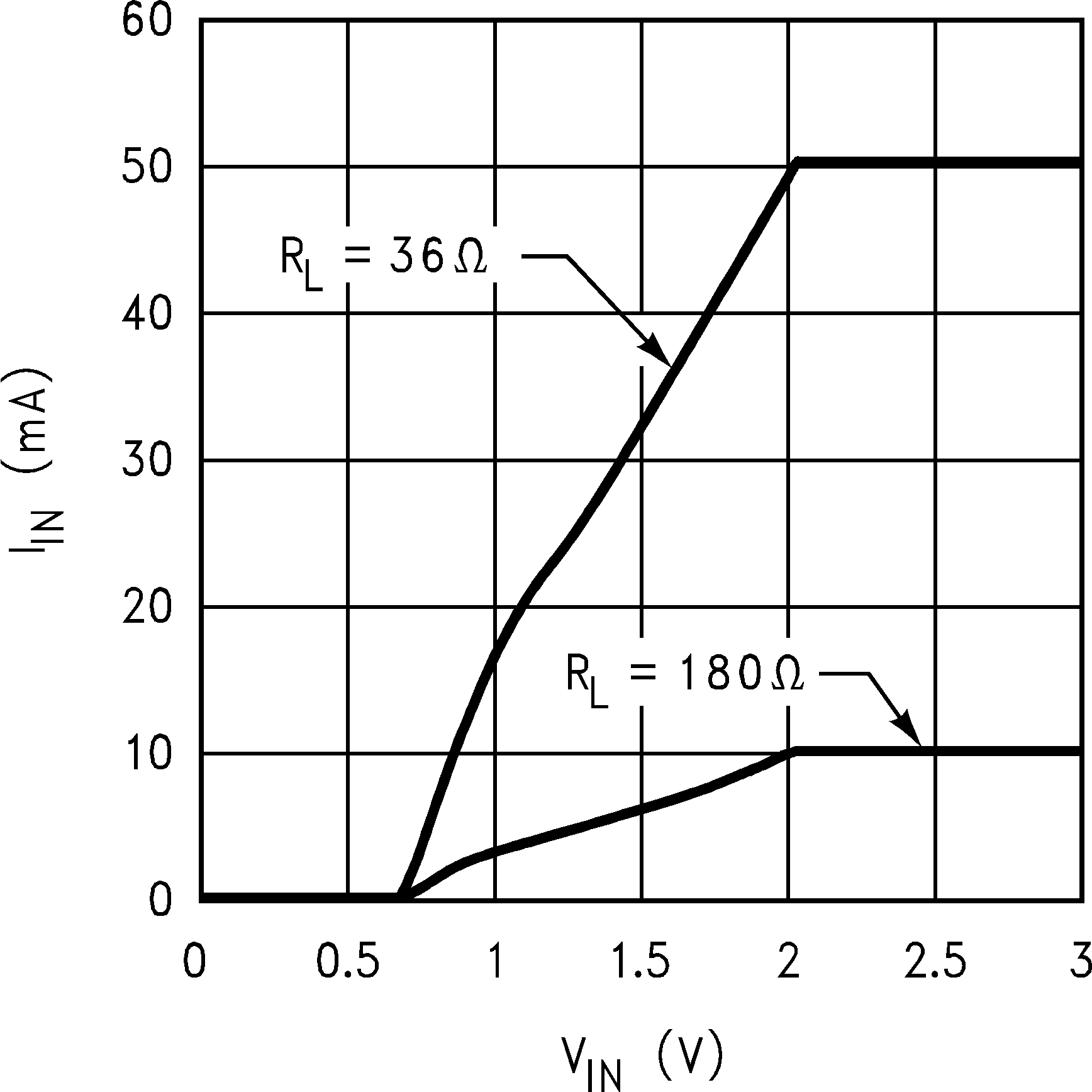 Figure 16. Input Current vs VIN
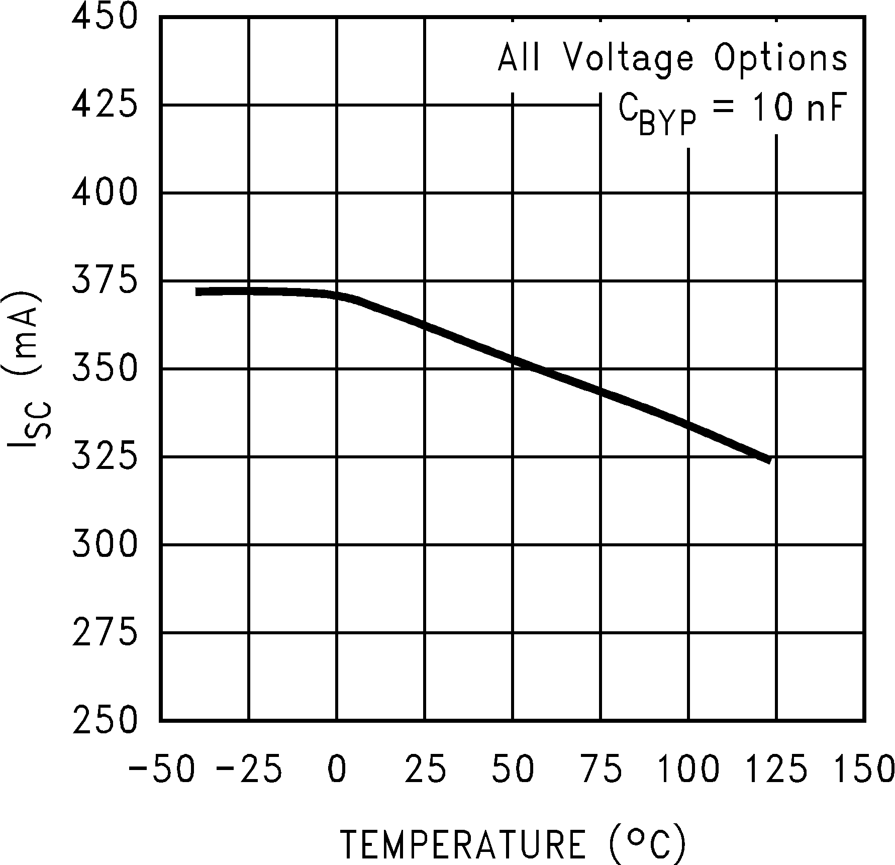 Figure 18. Instantaneous Short Circuit Current