JAJS700Q November 1999 – October 2016 LP2985LV-N
PRODUCTION DATA.
- 1 特長
- 2 アプリケーション
- 3 概要
- 4 改訂履歴
- 5 Pin Configuration and Functions
- 6 Specifications
- 7 Detailed Description
-
8 Application and Implementation
- 8.1 Application Information
- 8.2 Typical Application
- 9 Power Supply Recommendations
- 10Layout
- 11デバイスおよびドキュメントのサポート
- 12メカニカル、パッケージ、および注文情報
8 Application and Implementation
NOTE
Information in the following applications sections is not part of the TI component specification, and TI does not warrant its accuracy or completeness. TI’s customers are responsible for determining suitability of components for their purposes. Customers should validate and test their design implementation to confirm system functionality.
8.1 Application Information
The LP2985LV-N is a linear voltage regulator operating from 2.2 V to 16 V on the input and regulating voltages from 1.5 V to 2 V with 1% accuracy (A-grade) and 150-mA maximum output current. Efficiency is defined by the ratio of output voltage to input voltage because the LP2985LV-N is a linear voltage regulator. To achieve high efficiency, the dropout voltage (VIN – VOUT) must be as small as possible, thus requiring a very-low-dropout LDO. Successfully implementing an LDO in an application depends on the application requirements. If the requirements are simply input voltage and output voltage, compliance specifications (such as internal power dissipation or stability) must be verified to ensure a solid design. If timing, start-up, noise, power supply rejection ratio (PSRR), or any other transient specification is required, then the design becomes more challenging.
8.2 Typical Application
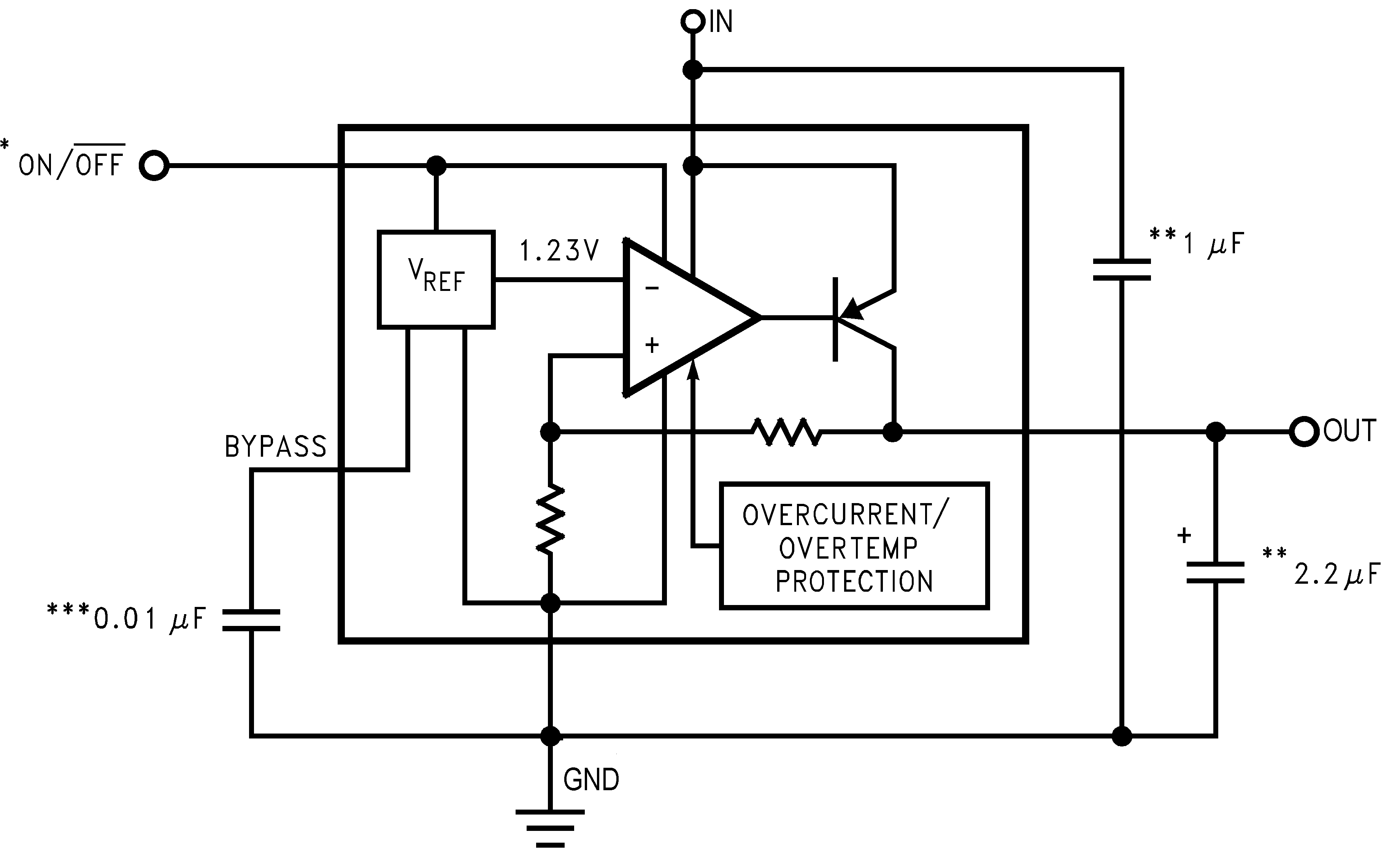
**Minimum capacitance is shown to ensure stability (may be increased without limit). Ceramic capacitor required for output (see Output Capacitor).
***Reduces output noise (may be omitted if application is not noise critical). Use ceramic or film type with very low leakage current (see Noise Bypass Capacitor).
8.2.1 Design Requirements
For typical design parameters, see Table 1.
Table 1. Design Parameters
| DESIGN PARAMETERS | VALUE |
|---|---|
| Input voltage | 2.8 V ±10% |
| Output voltage | 1.8 V ±4% |
| Output current | 150 mA (maximum) |
| PSRR at 1 kHz | > 50 dB |
8.2.2 Detailed Design Procedure
At 150-mA loading, the dropout of the LP2985LV-N has 600-mV maximum dropout over temperature, thus an 1000-mV headroom is sufficient for operation over both input and output voltage accuracy. The efficiency of the LP2985LV-N in this configuration is VOUT / VIN = 64%. To achieve the smallest form factor, the DSBGA package is selected.
Input and output capacitors are selected in accordance with the Capacitor Characteristics section. Ceramic capacitances of 1 μF for the input and one 2.2-μF capacitor for the output are selected. With a VIN of 2.8 V, a VOUT of 1.8 V, and an output current of 150 mA Equation 1 shows the power dissipation to be 150 mW. With an RθJA rating of 178.8°C/W for the DSBGA YPB package, and a maximum operating ambient temperature of 85°C, Equation 2 shows the maximum junction temperature to be approximately 111.8°C.
8.2.2.1 External Capacitors
Like any low-dropout regulator, the LP2985LV-N requires external capacitors for regulator stability. These capacitors must be correctly selected for good performance.
8.2.2.1.1 Input Capacitor
An input capacitor whose capacitance is ≥ 1 µF is required between the LP2985LV-N input and ground (the amount of capacitance may be increased without limit).
This capacitor must be located a distance of not more than 1 cm from the input pin and returned to a clean analog ground. Any good quality ceramic, tantalum, or film capacitor may be used at the input.
NOTE
Tantalum capacitors can suffer catastrophic failure due to surge current when connected to a low-impedance source of power (like a battery or very large capacitor). If a Tantalum capacitor is used at the input, it must be ensured by the manufacturer to have a surge current rating sufficient for the application.
There are no requirements for ESR on the input capacitor, but tolerance and temperature coefficient must be considered when selecting the capacitor to ensure the capacitance is ≥ 1 µF over the entire operating temperature range.
8.2.2.1.2 Output Capacitor
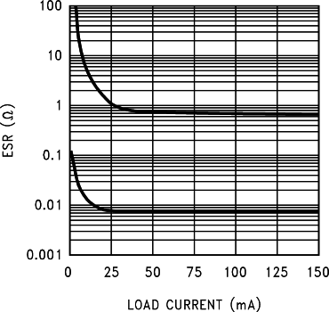
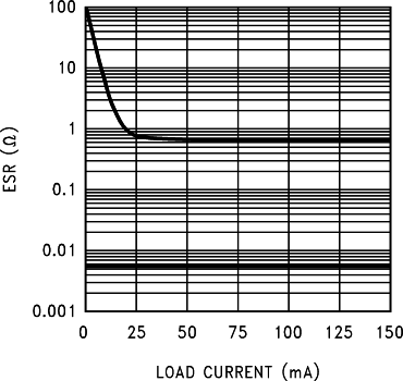
The LP2985LV-N is designed specifically to work with ceramic output capacitors, utilizing circuitry which allows the regulator to be stable across the entire range of output current with an output capacitor whose ESR is as low as 5 mΩ. It may also be possible to use tantalum or film capacitors at the output, but these are not as attractive for reasons of size and cost (see Capacitor Characteristics).
The output capacitor must meet the requirement for minimum amount of capacitance and also have an ESR value which is within the stable range. Curves are provided showing the stable ESR range as a function of load current (see Figure 21 and Figure 22).
NOTE
The output capacitor must maintain its ESR within the stable region over the full operating temperature range of the application to assure stability.
The LP2985LV-N requires a minimum of 2.2 µF on the output (output capacitor size can be increased without limit).
It is important to remember that capacitor tolerance and variation with temperature must be taken into consideration when selecting an output capacitor so that the minimum required amount of output capacitance is provided over the full operating temperature range. Ceramic capacitors can exhibit large changes in capacitance with temperature (see Capacitor Characteristics). The output capacitor must be located not more than 1 cm from the output pin and returned to a clean analog ground.
8.2.2.1.3 Noise Bypass Capacitor
Connecting a 10-nF capacitor to the BYPASS pin significantly reduces noise on the regulator output. The capacitor is connected directly to a high-impedance circuit in the bandgap reference.
Because this circuit has only a few microamperes flowing in it, any significant loading on this node causes a change in the regulated output voltage. For this reason, DC leakage current through the noise bypass capacitor must never exceed 100 nA and must be kept as low as possible for best output voltage accuracy.
The types of capacitors best suited for the noise bypass capacitor are ceramic and film. High-quality ceramic capacitors with either NPO or COG dielectric typically have very low leakage. 10-nF polypropolene and polycarbonate film capacitors are available in small surface-mount packages and typically have extremely low leakage current.
8.2.2.2 Capacitor Characteristics
The LP2985LV-N is designed to work with ceramic capacitors on the output to take advantage of the benefits they offer: for capacitance values in the 2.2-µF to 4.7-µF range, ceramics are the least expensive and also have the lowest ESR values (making them best for eliminating high-frequency noise). The ESR of a typical 2.2-µF ceramic capacitor is in the range of 10 mΩ to 20 mΩ, which easily meets the ESR limits required for stability by the device.
One disadvantage of ceramic capacitors is that their capacitance can vary with temperature. Most large value ceramic capacitors (≥ 2.2 µF) are manufactured with the Z5U or Y5V temperature characteristic, which results in the capacitance dropping by more than 50% as the temperature goes from 25°C to 85°C.
Problems may ensue if a 2.2-µF capacitor is used on the output because it drops down to approximately 1 µF at high ambient temperatures (which could cause the LM2985 to oscillate). If Z5U or Y5V capacitors are used on the output, a minimum capacitance value of 4.7 µF must be observed.
A better choice for temperature coefficient in ceramic capacitors is X7R, which holds the capacitance within ±15%. Unfortunately, the larger values of capacitance are not offered by all manufacturers in the X7R dielectric.
8.2.2.2.1 Tantalum
Tantalum capacitors are less desirable than ceramics for use as output capacitors because they are more expensive when comparing equivalent capacitance and voltage ratings in the 1 µF to 4.7 µF range.
An additional important consideration is that tantalum capacitors have higher ESR values than equivalent size ceramics. This means that while it may be possible to find a tantalum capacitor with an ESR value within the stable range, it would have to be larger in capacitance (which means bigger and more costly) than a ceramic capacitor with the same ESR value.
Note that the ESR of a typical tantalum increases about 2:1 as the temperature goes from 25°C down to −40°C, so some guard band must be allowed.
8.2.2.3 On/OFF Input Operation
The LP2985LV-N is shut off by driving the ON/OFF input low, and turned on by pulling it high. If this feature is not to be used, the ON/OFF input must be tied to VIN to keep the regulator output on at all times.
To assure proper operation, the signal source used to drive the ON/OFF input must be able to swing above and below the specified turnon/turnoff voltage thresholds listed inElectrical Characteristics under VON/OFF. To prevent mis-operation, the turnon (and turnoff) voltage signals applied to the ON/OFF input must have a slew rate which is ≥ 40 mV/µs.
CAUTION
The regulator output voltage cannot be ensured if a slow-moving AC (or DC) signal is applied that is in the range between the specified turnon and turnoff voltages listed under the electrical specification VON/OFF (see Electrical Characteristics).
8.2.2.4 Reverse Input-Output Voltage
The PNP power transistor used as the pass element in the LP2985LV-N has an inherent diode connected between the regulator output and input. During normal operation (where the input voltage is higher than the output) this diode is reverse-biased.
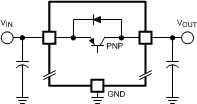 Figure 23. Normal Operation
However, if the output is pulled above the input, this diode turns ON, and current flows into the regulator output. In such cases, a parasitic SCR can latch, allowing a high current to flow into VIN (and out the ground pin), which can damage the part.
In any application where the output may be pulled above the input, an external Schottky diode must be connected from VIN to VOUT (cathode on VIN, anode on VOUT), to limit the reverse voltage across the LP2985LV-N to 0.3V (see Absolute Maximum Ratings).
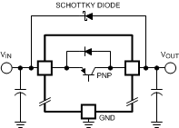 Figure 24. Operation With Schottky Diode
8.2.2.5 Power Dissipation
Knowing the device power dissipation and proper sizing of the thermal plane connected to the tab or pad is critical to ensuring reliable operation. Device power dissipation depends on input voltage, output voltage, and load conditions and can be calculated with Equation 1.
Power dissipation can be minimized, and greater efficiency can be achieved, by using the lowest available voltage drop option that would still be greater than the dropout voltage (VDO). However, keep in mind that higher voltage drops result in better dynamic (that is, PSRR and transient) performance.
On the DSBGA (YPB) package, the primary conduction path for heat is through the four bumps to the PCB.
On the SOT-23 (DBV) package, the primary conduction path for heat is through the device leads to the PCB, predominately device lead 2 (GND). It is recommended that the trace from lead 2 be extended under the package body and connected to an internal ground plane with thermal vias.
The maximum allowable junction temperature (TJ(MAX)) determines maximum power dissipation allowed (PD(MAX)) for the device package.
Power dissipation and junction temperature are most often related by the junction-to-ambient thermal resistance (RθJA) of the combined PCB and device package and the temperature of the ambient air (TA), according to Equation 2 or Equation 3:
Unfortunately, this RθJA is highly dependent on the heat-spreading capability of the particular PCB design, and therefore varies according to the total copper area, copper weight, and location of the planes. The RθJA recorded in Thermal Information is determined by the specific EIA/JEDEC JESD51-7 standard for PCB and copper-spreading area, and is to be used only as a relative measure of package thermal performance. For a well-designed thermal layout, RθJA is actually the sum of the package junction-to-case (bottom) thermal resistance (RθJCbot) plus the thermal resistance contribution by the PCB copper area acting as a heat sink.
8.2.2.6 Estimating Junction Temperature
The EIA/JEDEC standard recommends the use of psi (Ψ) thermal characteristics to estimate the junction temperatures of surface mount devices on a typical PCB board application. These characteristics are not true thermal resistance values, but rather package specific thermal characteristics that offer practical and relative means of estimating junction temperatures. These psi metrics are determined to be significantly independent of copper-spreading area. The key thermal characteristics (ΨJT and ΨJB) are given in Thermal Information and are used in accordance with Equation 4 or Equation 5.
where
- PD(MAX) is explained in Equation 1.
- TTOP is the temperature measured at the center-top of the device package.
where
- PD(MAX) is explained in Equation 1.
- TBOARD is the PCB surface temperature measured 1-mm from the device package and centered on the package edge.
For more information about the thermal characteristics ΨJT and ΨJB, see Semiconductor and IC Package Thermal Metrics, available for download at www.ti.com.
For more information about measuring TTOP and TBOARD, see Using New Thermal Metrics, available for download at www.ti.com.
For more information about the EIA/JEDEC JESD51 PCB used for validating RθJA, see Thermal Characteristics of Linear and Logic Packages Using JEDEC PCB Designs, available for download at www.ti.com.
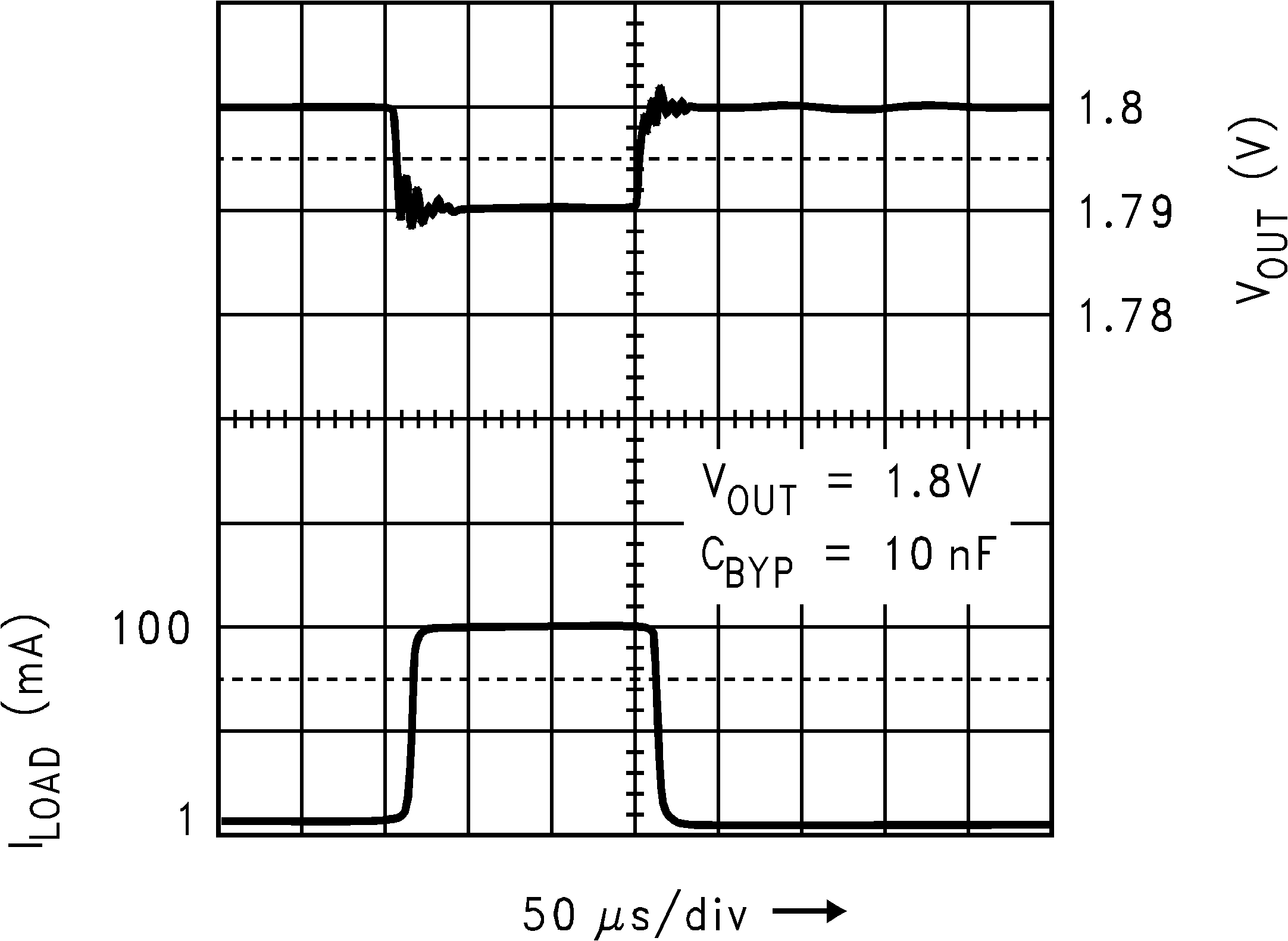
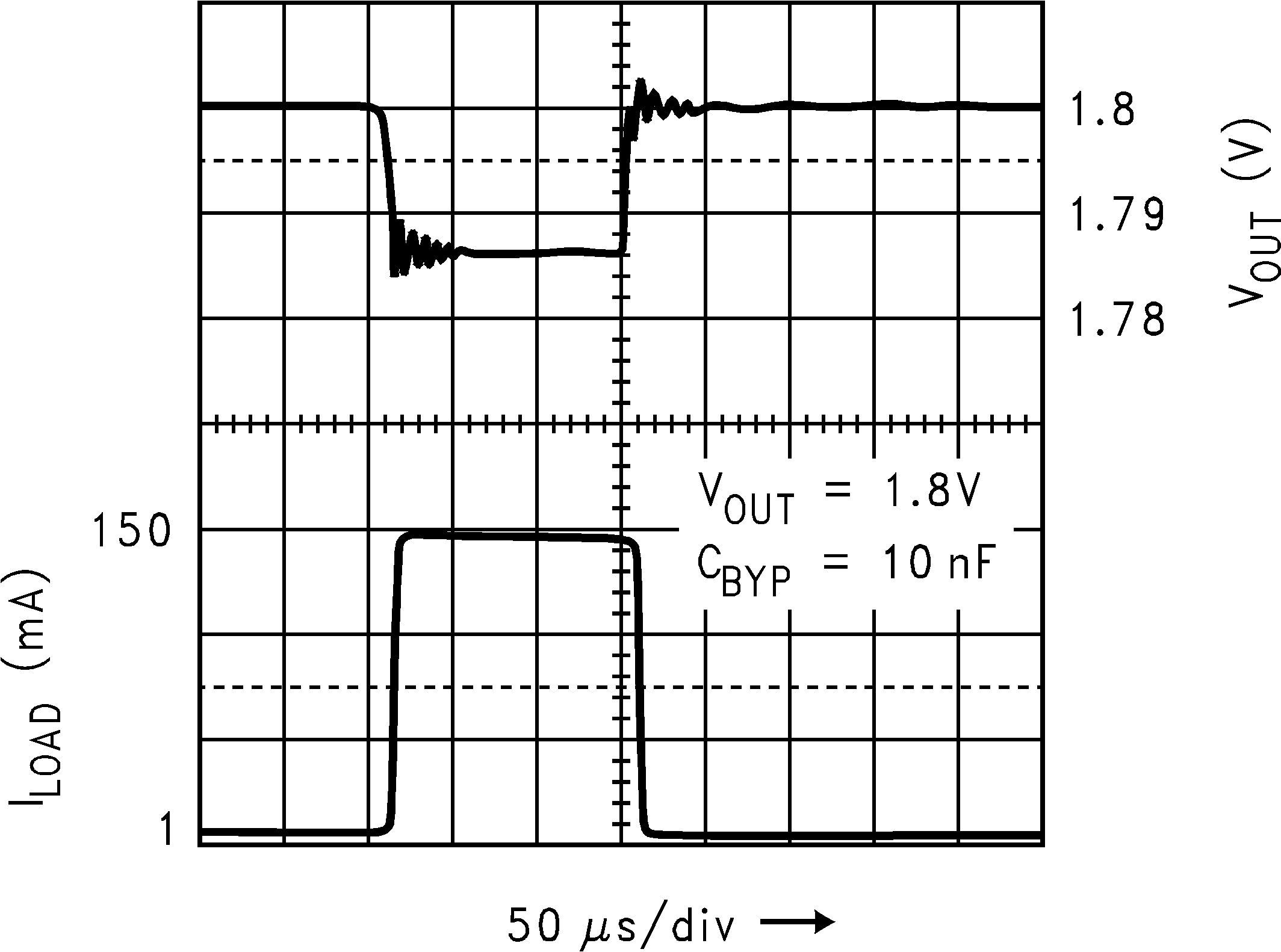
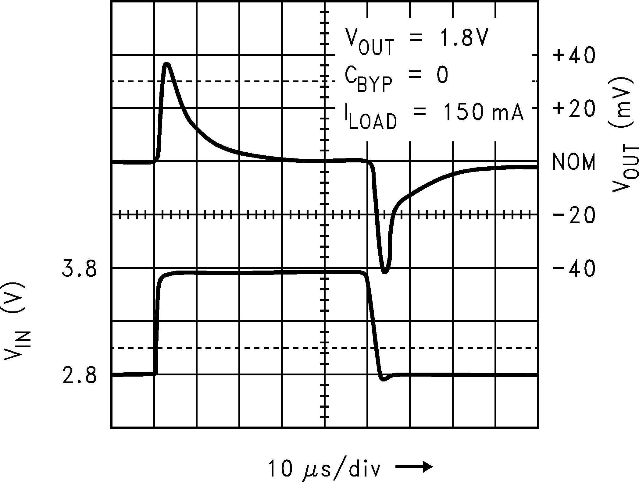
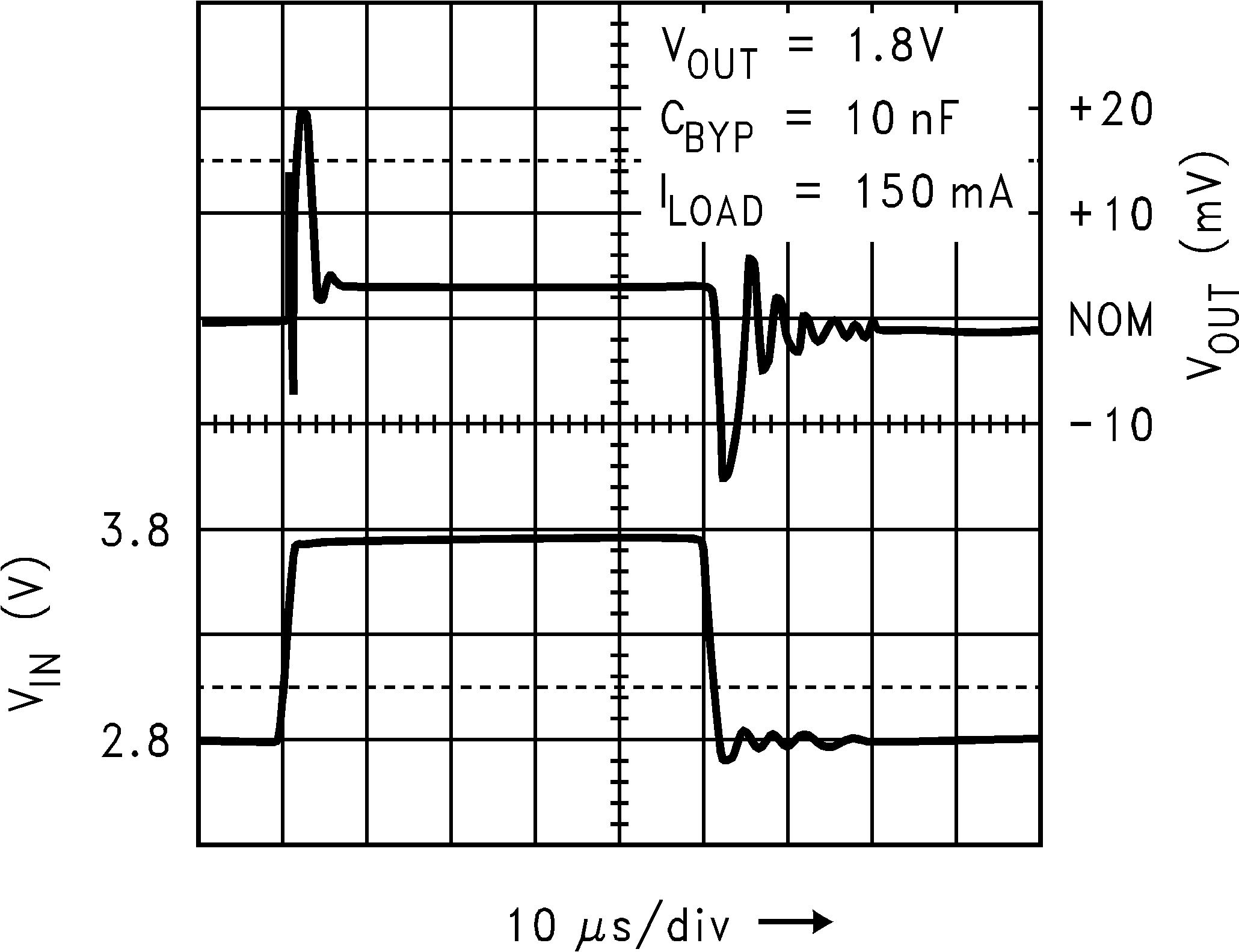
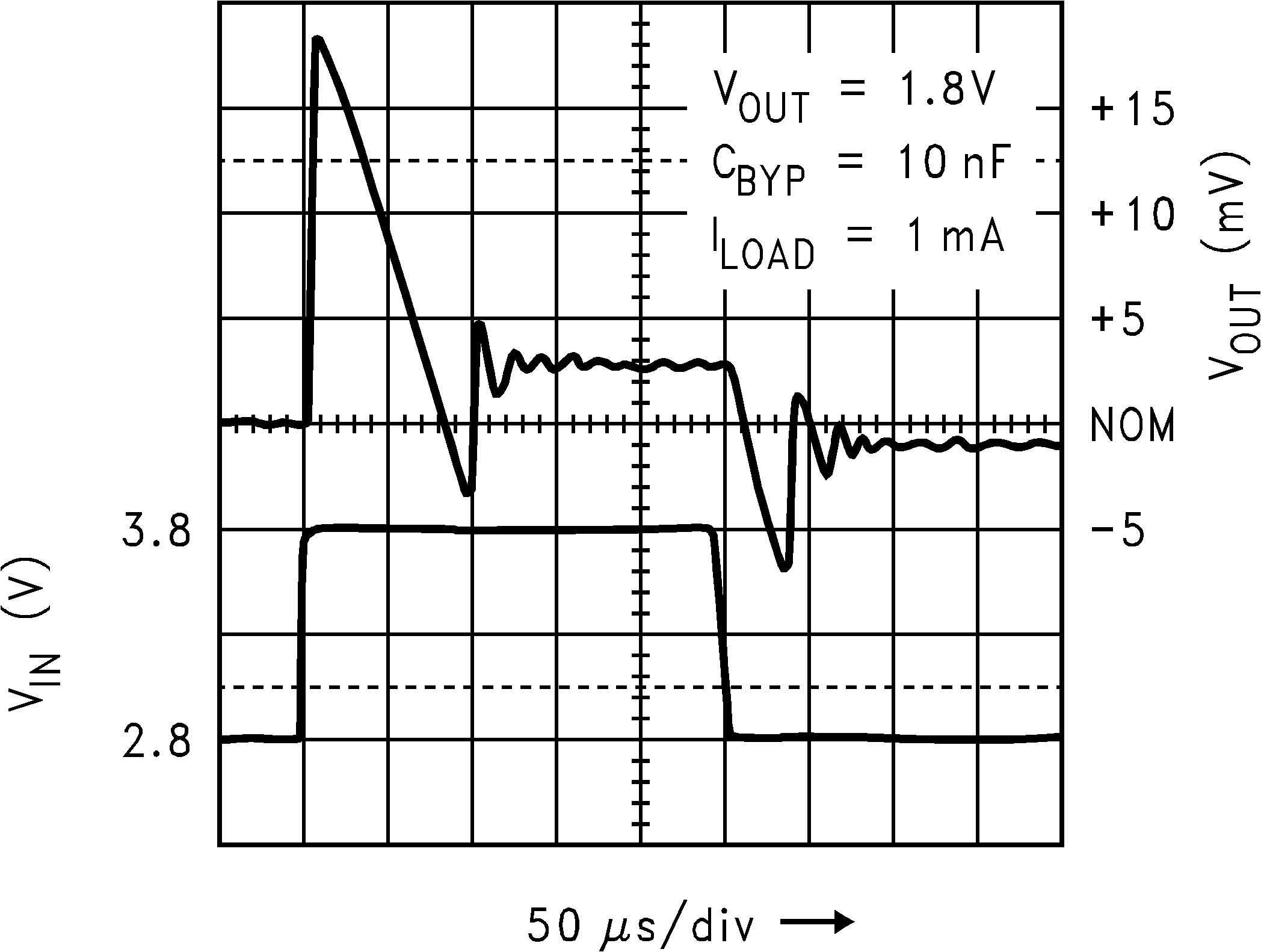
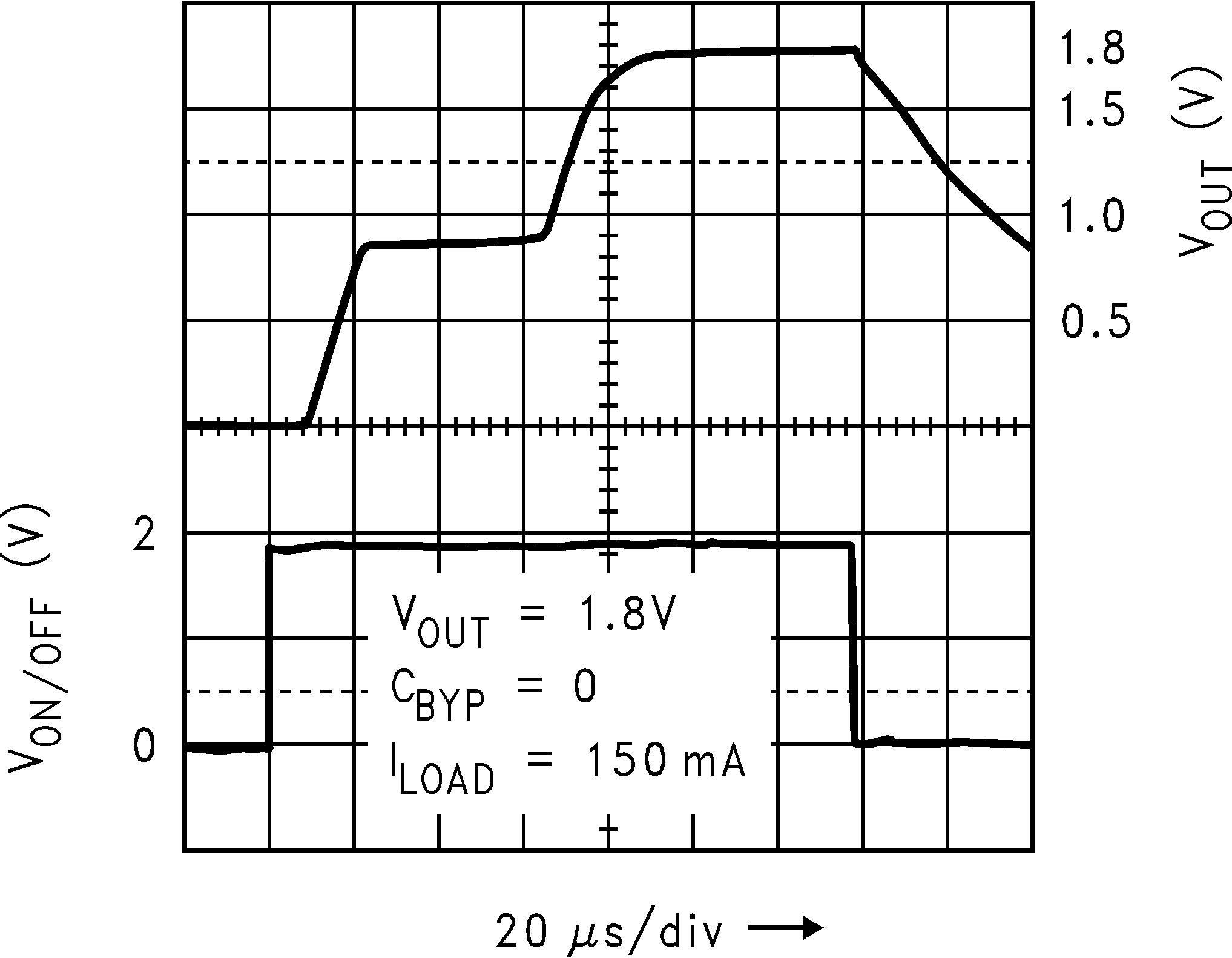
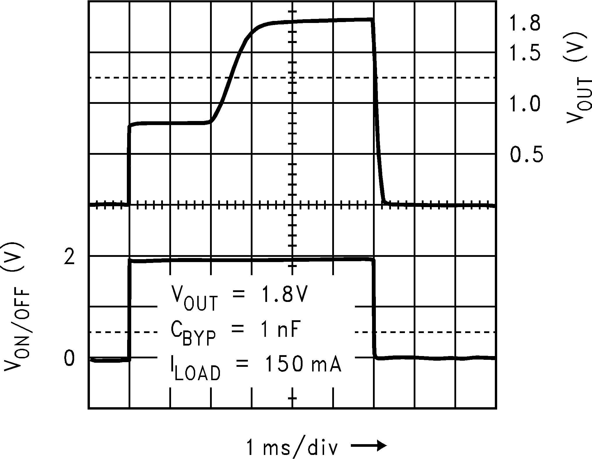
8.2.3 Application Curves
