JAJSG64C March 2015 – August 2018 LP8758-B0
PRODUCTION DATA.
- 1 特長
- 2 アプリケーション
- 3 概要
- 4 概略回路図
- 5 改訂履歴
- 6 Pin Configuration and Functions
- 7 Specifications
-
8 Detailed Description
- 8.1 Overview
- 8.2 Functional Block Diagram
- 8.3 Feature Description
- 8.4 Device Functional Modes
- 8.5 Programming
- 8.6
Register Maps
- 8.6.1
Register Descriptions
- 8.6.1.1 DEV_REV
- 8.6.1.2 OTP_REV
- 8.6.1.3 BUCK0_CTRL1
- 8.6.1.4 BUCK0_CTRL2
- 8.6.1.5 BUCK1_CTRL2
- 8.6.1.6 BUCK2_CTRL2
- 8.6.1.7 BUCK3_CTRL2
- 8.6.1.8 BUCK0_VOUT
- 8.6.1.9 BUCK0_FLOOR_VOUT
- 8.6.1.10 BUCK0_DELAY
- 8.6.1.11 RESET
- 8.6.1.12 CONFIG
- 8.6.1.13 INT_TOP
- 8.6.1.14 INT_BUCK_0_1
- 8.6.1.15 INT_BUCK_2_3
- 8.6.1.16 TOP_STAT
- 8.6.1.17 BUCK_0_1_STAT
- 8.6.1.18 BUCK_2_3_STAT
- 8.6.1.19 TOP_MASK
- 8.6.1.20 BUCK_0_1_MASK
- 8.6.1.21 BUCK_2_3_MASK
- 8.6.1.22 SEL_I_LOAD
- 8.6.1.23 I_LOAD_2
- 8.6.1.24 I_LOAD_1
- 8.6.1
Register Descriptions
- 9 Application and Implementation
- 10Power Supply Recommendations
- 11Layout
- 12デバイスおよびドキュメントのサポート
- 13メカニカル、パッケージ、および注文情報
8.3.3.1 Enabling and Disabling Regulator
The regulator can be enabled when the device is in STANDBY state. There are two ways for enable and disable the regulator:
- Using BUCK0_CTRL1.EN_BUCK0 register bit (BUCK0_CTRL1.EN_PIN_CTRL0 register bit is '0').
- Using EN1/2 control pins (BUCK0_CTRL1.EN_BUCK0 register bit is '1' AND
BUCK0_CTRL1.EN_PIN_CTRL0 register bit is '1').
If the EN1/2 control pins are used for enable and disable then the delay from the control signal rising edge to startup is set by BUCK0_DELAY.BUCK0_STARTUP_DELAY[3:0] bits and the delay from control signal falling edge to shutdown is set by BUCK0_DELAY.BUCK0_SHUTDOWN_DELAY[3:0] bits. The delays are valid only for EN1/2 signal and not for control with BUCK0_CTRL1.EN_BUCK0 bit. The delay time implemented by EN1/2 has overall +/-10% timing accuracy.
The control of the regulator (with 0 ms delays) is shown in Table 1. The multi-phase regulator is controlled with registers of the master phase.
Table 1. Regulator Control
| CONTROL METHOD | ROW | EN_BUCKx0 | BUCK0_CTRL1
EN_PIN_CTRL0 |
BUCK0_CTRL1
EN_PIN_SELECT0 |
BUCK0_CTRL1
EN_ROOF_FLOOR0 |
EN1 PIN | EN2 PIN | BUCK0
OUTPUT VOLTAGE |
|---|---|---|---|---|---|---|---|---|
| Enable/disable control with EN_BUCK0 bit | 1 | 0 | Don't Care | Don't Care | Don't Care | Don't Care | Don't Care | Disabled |
| 2 | 1 | 0 | Don't Care | Don't Care | Don't Care | Don't Care | BUCK0_VOUT.BUCK0_VSET[7:0] | |
| Enable/disable control with EN1 pin | 3 | 1 | 1 | 0 | 0 | Low | Don't Care | Disabled |
| 4 | 1 | 1 | 0 | 0 | High | Don't Care | BUCK0_VOUT.BUCK0_VSET[7:0] | |
| Enable/disable control with EN2 pin | 5 | 1 | 1 | 1 | 0 | Don't Care | Low | Disabled |
| 6 | 1 | 1 | 1 | 0 | Don't Care | High | BUCK0_VOUT.BUCK0_VSET[7:0] | |
| Roof/floor control with EN1 pin | 7 | 1 | 1 | 0 | 1 | Low | Don't Care | BUCK0_FLOOR_VOUT.BUCK0_FLOOR_VSET[7:0] |
| 8 | 1 | 1 | 0 | 1 | High | Don't Care | BUCK0_VOUT.BUCK0_VSET[7:0] | |
| Roof/floor control with EN2 pin | 9 | 1 | 1 | 1 | 1 | Don't Care | Low | BUCK0_FLOOR_VOUT.BUCK0_FLOOR_VSET[7:0] |
| 10 | 1 | 1 | 1 | 1 | Don't Care | High | BUCK0_VOUT.BUCK0_VSET[7:0] |
The following configuration allows the enable/disable control using ENx pin:
- BUCK0_CTRL1.EN_BUCK0 = 1
- BUCK0_CTRL1.EN_PIN_CTRL0 = 1
- BUCK0_CTRL1.EN_ROOF_FLOOR0 = 0
- BUCK0_VOUT.BUCK0_VSET[7:0] = Required voltage when ENx is high
- The enable pin for control is selected with BUCK0_CTRL1.EN_PIN_SELECT0
When the ENx pin is low, Table 1 row 3 (or 5) is valid, and the regulator is disabled. By setting ENx pin high, Table 1 row 4 (or 6) is valid, and the regulator is enabled with required voltage.
If the regulator is enabled all the time, and the ENx pin controls selection between two voltage level, the following configuration is used:
- BUCK0_CTRL1.EN_BUCK0 = 1
- BUCK0_CTRL1.EN_PIN_CTRL0 = 1
- BUCK0_CTRL1.EN_ROOF_FLOOR0 = 1
- BUCK0_VOUT.BUCK0_VSET[7:0] = Required voltage when ENx is high
- The enable pin for control is selected with BUCK0_CTRL1.EN_PIN_SELECT0
When the ENx pin is low, Table 1 row 7(or 9) is valid, and the regulator is enabled with a voltage defined by BUCK0_FLOOR_VOUT.BUCK0_FLOOR_VSET[7:0] bits. Setting the ENx pin high, Table 1 row 8 (or 10) is valid, and the regulator is enabled with a voltage defined by BUCK0_VOUT.BUCK0_VSET[7:0] bits.
If the regulator is controlled by I2C writings, the BUCK0_CTRL1.EN_PIN_CTRL0 bit is set to 0. The enable/disable is controlled by the BUCK0_CTRL1.EN_BUCK0 bit, and when the regulator is enabled, the output voltage is defined by the BUCK0_VOUT.BUCK0_VSET[7:0] bits. The Table 1 rows 1 and 2 are valid for I2C controlled operation (ENx pins are ignored).
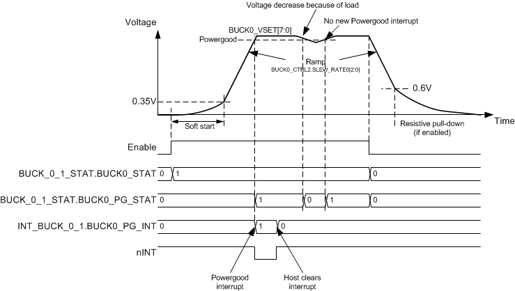
The regulator is enabled by the ENx pin or by I2C writing as shown in Figure 11. The soft-start circuit limits the in-rush current during start-up. Output voltage increase rate is around 30 mV/μsec during soft-start. When the output voltage rises to approximately 0.3 V, the output voltage becomes slew-rate controlled. If there is a short circuit at the output, and the output voltage does not increase above a 0.35-V level in 1 ms, the regulator is disabled, and interrupt is set. When the output voltage reaches the powergood threshold level the INT_BUCK_0_1.BUCK0_PG_INT interrupt flag is set. The powergood interrupt flag can be masked using BUCK_0_1_MASK.BUCK0_PG_MASK bit.
The ENx input pins have integrated pull-down resistors. The pull-down resistors are enabled by default and host can disable those with CONFIG.ENx_PD bits.
 Figure 11. Regulator Enable and Disable