JAJSD62C March   2013  – January 2020 OPA188

PRODUCTION DATA.  

  1. 特長
  2. アプリケーション
  3. 概要
    1.     Device Images
      1.      自動ゼロ化技術による、非常に低い温度ドリフト係数の実現
  4. 改訂履歴
  5. Device Comparison Table
    1. 5.1 Portfolio Comparison
  6. Pin Configuration and Functions
    1.     Pin Functions
  7. Specifications
    1. 7.1 Absolute Maximum Ratings
    2. 7.2 ESD Ratings
    3. 7.3 Recommended Operating Conditions
    4. 7.4 Thermal Information
    5. 7.5 Electrical Characteristics: High-Voltage Operation
    6. 7.6 Electrical Characteristics: Low-Voltage Operation
    7. 7.7 Typical Characteristics: Table of Graphs
      1. 7.7.1 Table of Graphs
    8. 7.8 Typical Characteristics
  8. Detailed Description
    1. 8.1 Overview
    2. 8.2 Functional Block Diagram
    3. 8.3 Feature Description
      1. 8.3.1 Operating Characteristics
      2. 8.3.2 Phase-Reversal Protection
      3. 8.3.3 Input Bias Current Clock Feedthrough
      4. 8.3.4 Internal Offset Correction
      5. 8.3.5 EMI Rejection
      6. 8.3.6 Capacitive Load and Stability
      7. 8.3.7 Electrical Overstress
    4. 8.4 Device Functional Modes
  9. Application and Implementation
    1. 9.1 Application Information
    2. 9.2 Typical Applications
      1. 9.2.1 High-Side Voltage-to-Current (V-I) Converter
        1. 9.2.1.1 Design Requirements
        2. 9.2.1.2 Detailed Design Procedure
        3. 9.2.1.3 Application Curves
      2. 9.2.2 Discrete INA + Attenuation for ADC With 3.3-V Supply
      3. 9.2.3 Bridge Amplifier
      4. 9.2.4 Low-Side Current Monitor
      5. 9.2.5 Programmable Power Supply
      6. 9.2.6 RTD Amplifier With Linearization
  10. 10Power Supply Recommendations
  11. 11Layout
    1. 11.1 Layout Guidelines
    2. 11.2 Layout Example
  12. 12デバイスおよびドキュメントのサポート
    1. 12.1 デバイス・サポート
      1. 12.1.1 開発サポート
        1. 12.1.1.1 TINA-TI(無償のダウンロード・ソフトウェア)
    2. 12.2 ドキュメントのサポート
      1. 12.2.1 関連資料
    3. 12.3 ドキュメントの更新通知を受け取る方法
    4. 12.4 サポート・リソース
    5. 12.5 商標
    6. 12.6 静電気放電に関する注意事項
    7. 12.7 Glossary
  13. 13メカニカル、パッケージ、および注文情報

パッケージ・オプション

メカニカル・データ(パッケージ|ピン)
サーマルパッド・メカニカル・データ
発注情報

Capacitive Load and Stability

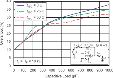
The device dynamic characteristics are optimized for a range of common operating conditions. The combination of low closed-loop gain and high capacitive loads decreases the amplifier phase margin and can lead to gain peaking or oscillations. As a result, larger capacitive loads must be isolated from the output. The simplest way to achieve this isolation is to add a small resistor (for example, ROUT equal to 50 Ω) in series with the output. Figure 41 and Figure 42 show graphs of small-signal overshoot versus capacitive load for several values of ROUT. For details of analysis techniques and application circuits, see Feedback Plots Define Op Amp AC Performance, available for download from www.ti.com.
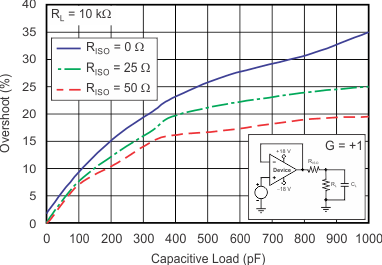
OPA188 tc_sm_oshoot-cl_pos_bos642.gif
G = 1 RL = 10 kΩ 100-mV Output Step
Figure 41. Small-Signal Overshoot vs Capacitive Load
OPA188 tc_sm_oshoot-cl_neg_bos642.gif
G = –1 RL = RF = 10 kΩ 100-mV Output Step
Figure 42. Small-Signal Overshoot vs Capacitive Load