JAJSS83A November 2023 – December 2023 REF54
PRODUCTION DATA
- 1
- 1 特長
- 2 アプリケーション
- 3 概要
- 4 Device Comparison Table
- 5 Pin Configuration and Functions
-
6 Specifications
- 6.1 Absolute Maximum Ratings
- 6.2 ESD Ratings
- 6.3 Recommended Operating Conditions
- 6.4 Thermal Information
- 6.5 Electrical Characteristics REF54250
- 6.6 Electrical Characteristics REF54300
- 6.7 Electrical Characteristics REF54410
- 6.8 Electrical Characteristics REF54450
- 6.9 Electrical Characteristics REF54500
- 6.10 Typical Characteristics
- 7 Parameter Measurement Information
- 8 Detailed Description
- 9 Application and Implementation
- 10Device and Documentation Support
- 11Revision History
- 12Mechanical, Packaging, and Orderable Information
7.4 Thermal Hysteresis
Thermal hysteresis is measured with the REF54 soldered to a PCB, similar to a real-world application. Thermal hysteresis for the device is defined as the change in output voltage after operating the device at 25°C, cycling the device through the specified temperature range, and returning to 25°C. The fist thermal cycle for C variant is shown in Figure 7-10 and second cycle is shown in Figure 7-11. Thermal hysteresis for REF54250CDR settles after first cycle. Hysteresis can be expressed by Equation 2
Equation 2. 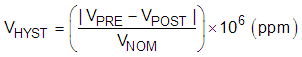
where
- VHYST = thermal hysteresis (in units of ppm)
- VNOM = the specified output voltage
- VPRE = output voltage measured at 25°C pre-temperature cycling
- VPOST = output voltage measured after the device has cycled from 25°C through the specified temperature range (eg. 0°C to 70°C ) and returns to 25°C.
 - Cycle 1") Figure 7-10 Thermal Hysteresis
Distribution
Figure 7-10 Thermal Hysteresis
Distribution (0°C to 70°C) - Cycle 1
 - Cycle 2") Figure 7-11 Thermal Hysteresis
Distribution
Figure 7-11 Thermal Hysteresis
Distribution (0°C to 70°C) - Cycle 2