JAJSS83A November 2023 – December 2023 REF54
PRODUCTION DATA
- 1
- 1 特長
- 2 アプリケーション
- 3 概要
- 4 Device Comparison Table
- 5 Pin Configuration and Functions
-
6 Specifications
- 6.1 Absolute Maximum Ratings
- 6.2 ESD Ratings
- 6.3 Recommended Operating Conditions
- 6.4 Thermal Information
- 6.5 Electrical Characteristics REF54250
- 6.6 Electrical Characteristics REF54300
- 6.7 Electrical Characteristics REF54410
- 6.8 Electrical Characteristics REF54450
- 6.9 Electrical Characteristics REF54500
- 6.10 Typical Characteristics
- 7 Parameter Measurement Information
- 8 Detailed Description
- 9 Application and Implementation
- 10Device and Documentation Support
- 11Revision History
- 12Mechanical, Packaging, and Orderable Information
7.6 Power Dissipation
The REF54 voltage references are capable of source and sink up to 10 mA of load current across the rated input voltage range. However, when used in applications subject to high ambient temperatures, the input voltage and load current must be carefully monitored to make sure that the device does not exceed the maximum power dissipation rating. The maximum power dissipation of the device can be calculated with Equation 3:
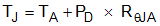
where
- PD is the device power dissipation
- TJ is the device junction temperature
- TA is the ambient temperature
- RθJA is the package (junction-to-air) thermal resistance
Because of this relationship, acceptable load current in high temperature conditions can be less than the maximum current-sourcing capability of the device. Do not operate the device outside of the maximum power rating because doing so can result in premature failure or permanent damage to the device.