JAJSC86B May 2016 – August 2016 REF6025 , REF6030 , REF6033 , REF6041 , REF6045 , REF6050
PRODUCTION DATA.
9 Detailed Description
9.1 Overview
Most SAR ADCs, and a few delta-sigma ADCs, switch binary-weighted capacitors onto the REF pin during the conversion process. The magnitude of the capacitance switched onto the REF pin during each conversion depends on the input signal to the ADC. If a voltage reference is directly connected to the REF pin of these ADCs, the reference voltage droops because of the dynamic input signal dependent load of the binary-weighted capacitors. Because the reference voltage droop now has input signal dependance, significant degradation in THD and linearity for the system occurs.
In order to support this dynamic load and preserve the ADC linearity, distortion and noise performance, the output of the voltage reference must be buffered with a low-output impedance (high-bandwidth) buffer. The REF60xx family of voltage references have an integrated low output impedance buffer that enables the user to directly drive the REF pin of a SAR ADC, while preserving ADC linearity and distortion. In addition, the total noise in the full bandwidth of the REF60xx is extremely low, thus preserving the noise performance of the ADC. Voltage-Reference Impact on Total Harmonic Distortion (SLYY097) correlates the effect of reference settling to ADC distortion, and how the REF60xx achieves lowest distortion with minimal components and lowest power consumption.
The output voltage of the REF60xx does not droop below 1 LSB (18-bit), even during the first conversion while driving the REF pin of the ADS8881. This feature is useful in burst-mode, event-triggered, equivalent-time sampling, and variable-sampling-rate data-acquisition systems. Functional Block Diagram shows a simplified schematic of the REF60xx.
9.2 Functional Block Diagram

9.3 Feature Description
9.3.1 Integrated ADC Drive Buffer
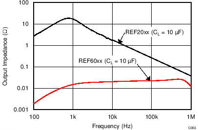
Many ADC data sheets specify a few microamps of average current draw from the REF pin. Almost all voltage references provide these few microamps of average current; but not all voltage references are practical for driving a high-resolution, high-throughput SAR ADC because the peak current drawn can be very high when the capacitors are switched on the REF pin. The worst-case demand for the voltage reference is during a burst-mode conversion, when the ADC is idle for a very long time, before a conversion is initiated, and the first sample converted is expected to be precise. Usually, a large capacitor is connected between the REF pin and ground pin (or sometimes between the REFP and REFM pins) of the ADC to smoothen the current load and reduce the burden on the voltage reference. The voltage reference must then be capable of providing the average current required to completely charge the reference capacitor, but without causing the reference voltage to droop significantly. Most voltage references lack the ability to completely charge the reference capacitor, and settle when the binary-weighted capacitors are being switched onto the REF pin because of the large output impedance. Usually, voltage references have output impedances in the range of 10's of ohms at frequencies higher than 100 Hz. The output voltage of the voltage reference must be buffered with a low output impedance (usually high bandwidth) amplifier to achieve excellent linearity and distortion performance.
The key amplifier specifications to be considered when designing a reference buffer for a high-precision ADC are: low offset, low drift, wide bandwidth, and low output impedance. While it is possible to select an amplifier that sufficiently meets all these requirements, the amplifier comes at a cost of excessive power consumption. For example, the OPA350 is a 38-MHz bandwidth amplifier with a maximum offset of 0.5 mV, and low offset drift of 4 µV/ºC, but consumes a quiescent current of 5.2mA. This is because (from an amplifier design perspective) offset and drift are dc specifications, whereas bandwidth, low output impedance, and high capacitive drive capability are high-frequency specifications. Therefore, achieving all the performance in one amplifier requires power. However, a more efficient design to meet the low power budget is to use a composite reference buffer, which uses an amplifier with superior high-frequency specifications in the feedback loop of a dc precision amplifier to get the overall performance at much lower power consumption. Figure 49 shows such a composite amplifier design with the OPA333 (dc precision amplifier) and THS4281 (high-bandwidth amplifier). This reference buffer design requires three devices, and a large number of external components. This solution still consumes close to 2 mA of quiescent current.
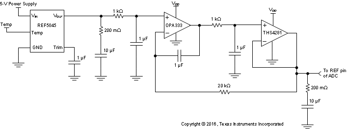 Figure 49. Composite Amplifier Reference Buffer
The REF60xx family of voltage references have an integrated low output impedance buffer (ADC drive buffer); therefore, there is no need for an external buffer while driving the REF pin of high-precision, high-throughput SAR ADCs, as shown in Figure 50. The ADC drive buffer of the REF60xx is capable of replenishing a charge of 70 pC on a 47-µF capacitor in 1 µs, without allowing the voltage on the capacitor to droop more than 1 LSB at 18-bit precision. The REF60xx are trimmed at multiple temperatures in production, achieving a max drift of just 5 ppm/°C for both the voltage reference and the buffer combined, while operating at a typical quiescent current of 820 µA. Figure 51 compares the output impedance of a regular voltage reference (REF20xx) and a voltage reference with integrated ADC drive buffer (REF60xx). Figure 52 compares the burst-mode, reference-settling performance of a regular voltage reference and the REF60xx.
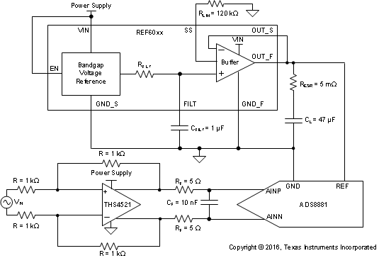 Figure 50. REF60xx Driving REF Pin of ADS8881 SAR ADC
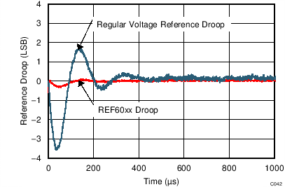
| 1 LSB = 19.07 µV, with ADS8881 at 1 MSPS |
9.3.2 Temperature Drift
The REF60xx family is designed for minimal drift error, defined as the change in output voltage over temperature. The drift is calculated using the box method, as described by the following equation:

9.3.3 Load Current
The REF6025, REF6030, REF6033 and REF6041 are specified to deliver current load of ±4 mA. The REF6045 is specified to deliver ±3.5 mA, and the REF6050 is specified to deliver ±3 mA. The REF60xx are protected from short circuits at the output by limiting the output short-circuit current.
The short-circuit current limit (ISC) of the REF60xx family of devices is adjusted by connecting a resistor (RSS) on the SS pin. The short-circuit current limit when the REF60xx device is sourcing current can be calculated as shown in Equation 4:

The short circuit current limit when the REF60xx device is sinking is calculated as shown in Equation 5:

The recommended output current of the REF60xx also depends on the resistor connected to the SS pin. The recommended output current (sourcing and sinking) for the REF6025, REF6030, REF6033 and REF6041 is given by Equation 6:

The recommended output current (sourcing and sinking) for the REF6045 is given by Equation 7:

The recommended output current (sourcing and sinking) for the REF6050 is given by Equation 8:

The temperature of the device increases according to Equation 9:

where
- TJ = junction temperature (°C).
- TA = ambient temperature (°C).
- PD = power dissipated (W).
- RθJA = junction-to-ambient thermal resistance (°C/W).
The REF60xx maximum junction temperature must not exceed the absolute maximum rating of 150°C.
9.3.4 Stability
The REF60xx family of voltage references are stable with output capacitor values ranging from 10 µF to 47 µF. At a low output-capacitor value of 10 µF, an effective series resistance (ESR) of 20 mΩ to 100 mΩ is required for stability; whereas, at a higher value of 47 µF, an ESR of 5 mΩ to 100 mΩ is required. The shaded region in Figure 53 shows the stable region of operation for the REF60xx devices.
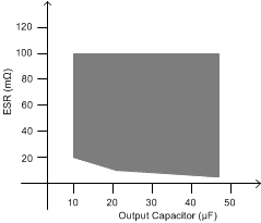 Figure 53. Stable Output Capacitor Range
A capacitor of value 1 µF is required at the FILT pin for stability and noise performance. A low ESR (5 mΩ to 20 mΩ) is easily achieved by increasing the PCB trace length, thus eliminating the need for a discrete resistor. Higher values of ESR (greater than 20 mΩ, but lesser than 100 mΩ) can be intentionally added to increase the output bandwidth of the REF60xx. This higher ESR improves the transient performance of the REF60xx, but worsens noise performance because of increased bandwidth.
9.4 Device Functional Modes
When the EN pin of the REF60xx is pulled high, the device is in active mode. The device must be in active mode for normal operation.
To place the REF60xx into a shutdown mode, pull the ENABLE pin low. When in shutdown mode, the output of the device becomes high impedance and the quiescent current of the device reduces to 1 µA (typ). See the enable pin voltage parameter in the Electrical Characteristics table for logic high and logic low voltage levels.