JAJSF58O MARCH 2001 – April 2018 SN65HVD230 , SN65HVD231 , SN65HVD232
PRODUCTION DATA.
- 1 特長
- 2 アプリケーション
- 3 概要
- 4 改訂履歴
- 5 概要(続き)
- 6 Device Comparison Table
- 7 Pin Configuration and Functions
-
8 Specifications
- 8.1 Absolute Maximum Ratings
- 8.2 ESD Ratings
- 8.3 Recommended Operating Conditions
- 8.4 Thermal Information
- 8.5 Electrical Characteristics: Driver
- 8.6 Electrical Characteristics: Receiver
- 8.7 Switching Characteristics: Driver
- 8.8 Switching Characteristics: Receiver
- 8.9 Switching Characteristics: Device
- 8.10 Device Control-Pin Characteristics
- 8.11 Typical Characteristics
- 9 Parameter Measurement Information
- 10Detailed Description
- 11Application and Implementation
- 12Power Supply Recommendations
- 13Layout
- 14デバイスおよびドキュメントのサポート
- 15メカニカル、パッケージ、および注文情報
11.2.1.2 Loop Propagation Delay
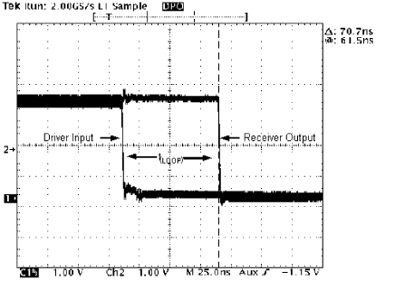
Transceiver loop delay is a measure of the overall device propagation delay, consisting of the delay from the driver input (D pin) to the differential outputs (CANH and CANL pins), plus the delay from the receiver inputs (CANH and CANL) to its output (R pin).
A typical loop delay for the SN65HVD230 transceiver is displayed in Figure 40. This loop delay will increase as the slope of the driver output is slowed during slope control mode. This increased loop delay means that there is a tradeoff between the total bus length able to be used and the driver's output slope used via the slope control pin of the device. For example, the loop delay for a 10-kΩ resistor from the RS pin to ground is ~100 ns, and the loop delay for a 100-kΩ resistor is ~500 ns. Therefore, if we use the following rule-of-thumb that the propagation delay of typical twisted pair bus cable is 5 ns/m, we can calculate an approximate cable length trade-off between normal high-speed mode and slope control mode with a 100-kΩ resistor. Using typical values, the loop delay for a recessive to dominant bit with RS tied directly to ground is 70ns, and with a 100-kΩ resistor is 535 ns. At 5ns/m of propagation delay, which you have to count in both directions the difference is 46.5 meters (535-70)/(2*5).
Another option to improving the elctromagnetic emissions of the device besides slowing down the edge rates of the driver in slope control mode is using quality shielded bus cabling.
 Figure 40. 70.7-ns Loop Delay Through the HVD230 With RS = 0