SLLS881G December 2007 – October 2014 SN65LVDS315
PRODUCTION DATA.
- 1 Features
- 2 Applications
- 3 Description
- 4 Revision History
- 5 Pin Configuration and Functions
- 6 Specifications
- 7 Parameter Measurement Information
-
8 Detailed Description
- 8.1 Overview
- 8.2 Functional Block Diagram
- 8.3
Feature Description
- 8.3.1 Frame Counter Size
- 8.3.2 Data Formats
- 8.3.3 Parallel Input Port Timing Information
- 8.3.4 MIPI CSI-1 / CCP2-Class 0 Interface
- 8.3.5 Frame Structure and Synchronization Codes
- 8.3.6 Preventing Wrong Synchronization
- 8.3.7 Frame Structure
- 8.3.8 VS and HS Timing to Generate the Correct Control Signals
- 8.4 Device Functional Modes
- 9 Application and Implementation
- 10Power Supply Recommendations
- 11Layout
- 12Device and Documentation Support
- 13Mechanical, Packaging, and Orderable Information
パッケージ・オプション
メカニカル・データ(パッケージ|ピン)
- RGE|24
サーマルパッド・メカニカル・データ
- RGE|24
発注情報
9 Application and Implementation
NOTE
Information in the following applications sections is not part of the TI component specification, and TI does not warrant its accuracy or completeness. TI’s customers are responsible for determining suitability of components for their purposes. Customers should validate and test their design implementation to confirm system functionality.
9.1 Application Information
The typical application for the SN65LVDS315 is the video streaming, where the device communicates the image sensor and the video processor, the SN65LVDS315 takes the video data from the image sensor in parallel format, then it serializes and sends this information in MIPI CSI-1.
9.1.1 Receiver Termination Requirement
The SN65LVDS315 outputs two differential lanes that must be specially terminated near the CSI-1 receiver device. As shown in Figure 25, place two resistors and one capacitor in each lane (within ±20% to the values shown). There are two possible implementations, based on whether the termination inside the receiver device can be disabled. If it can be disabled, place the components as close to the receiver as possible. This RC filter is a requirement that adds stability to the common mode voltage.
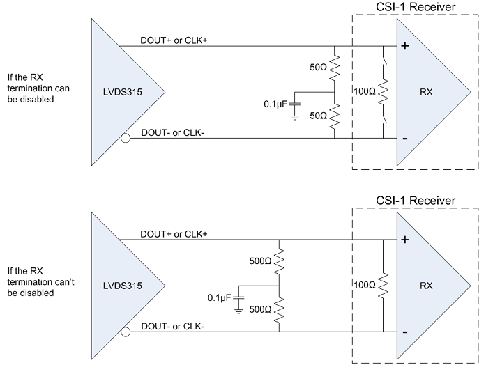 Figure 25. CSI-1 Receiver Device Termination
9.1.2 Preventing Control Inputs From Increased Leakage Currents
To ensure the lowest possible leakage current during standby or power down, all inputs must be held static. Any kind of input switching will cause increased leakage current. Hold inputs TXEN and MODE either at VIH or VIL. The LVDS315 incorporates a bus-hold feature on the D[0:7] inputs, DCLK, VS, and HS. This feature ensures that the input-stage leakage current is minimized during times when the camera output is in a high impedance state. Inputs with the bus-hold feature can be left open without the need of an external pullup or pulldown. This feature minimizes the power consumption of standby and power down modes in particular.
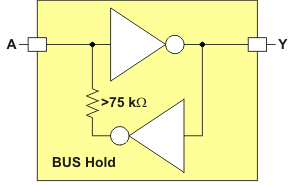 Figure 26. Bus-Hold Circuit
9.2 Typical Application
9.2.1 VGA Camera Application
Figure 27 shows a possible implementation of a 10-Mpixel camera transfer with 30Hz frame refresh rate. The SN65LVDS315 interfaces to the OMAP2420, a TI application processor with integrated CSI receiver. The pixel clock rate is 11 MHz, assuming ≈20% blanking overhead. The application assumes 8-bit color resolution.
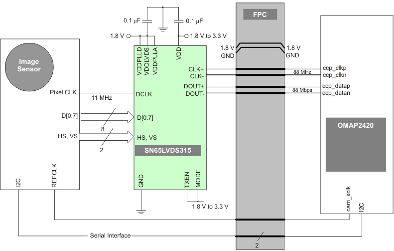 Figure 27. Typical VGA Display Application
9.2.1.1 Design Requirements
| PARAMETERS | VALUE |
|---|---|
| VDD supply voltage | 1.8 V to 3.3 V |
| VDDPLLD, VDDPLLA & VDDLVDS supply voltage | 1.8 V |
| Input frequency | 3.5 to 27 MHz (fixed to 11 MHz) |
| 8-bit parallel input data | YUV422, YUV420, RGB888, RGB565 & RAW8 |
| Input clock period jitter | 5 ps-rms |
9.2.1.2 Detailed Design Procedure
9.2.1.2.1 Calculation Example: VGA Camera Sensor
The following calculation shows an example for a VGA camera with following parameter:
| display resolution: | 640 x 480 |
| frame refresh rate: | 30 fps |
| vertical visible pixel: | 480 lines |
| vertical blanking: | 10 lines |
| horizontal visible pixel: | 640 columns |
| horizontal blanking: | 5 columns |
 Figure 28. VGA - Full Frame Composition
| Calculation of the total number of pixel and Blanking overhead: | |
| visible area pixel count: | 640 x 480 = 307,200 pixel |
| total frame pixel count: | (640+5) x (480+10) = 316,050 pixel |
| blanking overhead: | (316,050–307,200) div 307,200 = 2.8% |
| The application requires following serial link parameters: | |
| pixel clk frequency: | fDCLK = 316.050 x 30 Hz = 9.5 MHz |
| DOUT serial data rate: | dR = fDCLK x8 = 76 Mbps |
| CLK output clock rate: | fCLK = f(dR) = 76 MHz |
9.2.1.2.2 Typical Application Frequencies
The SN65LVDS315 in display mode supports pixel clock frequencies from 7 MHz to 27 MHz (which translates to DCLK frequencies of 56 MHz to 208 MHz). Table 7 provides a few typical display resolution examples. Table 7 also shows the assumed blanking overhead, which often times is smaller in the final application, resulting in a lower data rate.
9.2.1.2.2.1 8-Bit Camera Application
Table 7. Typical Application Data Rates And Serial Lane Usage
| DISPLAY SCREEN RESOLUTION | VISIBLE PIXEL COUNT | CONTROL OVERHEAD | FRAME REFRESH RATE | DCLK PIXEL CLOCK FREQUENCY [MHz] | DATA RATE ON D0 WITH LS=0 | f(CLK) |
|---|---|---|---|---|---|---|
| 640x480 (VGA) | 307,200 | 14% | 10 Hz | 3.5 MHz | 28 Mbps | 28 MHz |
| 640x480 (VGA) | 307,200 | 2% | 15 Hz | 4.7 MHz | 38 Mbps | 38 MHz |
| 640x480 (VGA) | 307,200 | 10% | 30 Hz | 10.1 MHz | 81 Mbps | 81 MHz |
| 3 Mpixel | 3,000,000 | 10% | 7 Hz | 23.1 MHz | 185 Mbps | 185 MHz |
| 4 Mpixel | 4,000,000 | 10% | 5 Hz | 22.0 MHz | 176 Mbps | 176 MHz |
| 5 Mpixel | 5,000,000 | 10% | 4 Hz | 22.0 MHz | 176 Mbps | 176 MHz |
| 6 Mpixel | 6,000,000 | 10% | 3 Hz | 19.8 MHz | 158 Mbps | 158 MHz |
| 8 Mpixel | 8,000,000 | 10% | 2 Hz | 17.6 MHz | 141 Mbps | 141 MHz |
| 10 Mpixel | 10,000,000 | 10% | 2 Hz | 22.0 MHz | 176 Mbps | 176 MHz |
| 12 Mpixel | 12,000,000 | 10% | 2 Hz | 25.1 MHz | 201 Mbps | 201 MHz |
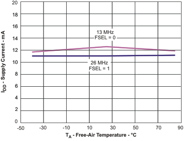
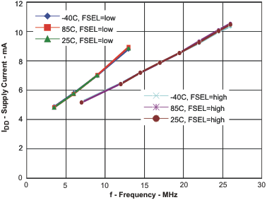
9.2.1.3 Application Curve