SLLS881G December 2007 – October 2014 SN65LVDS315
PRODUCTION DATA.
- 1 Features
- 2 Applications
- 3 Description
- 4 Revision History
- 5 Pin Configuration and Functions
- 6 Specifications
- 7 Parameter Measurement Information
-
8 Detailed Description
- 8.1 Overview
- 8.2 Functional Block Diagram
- 8.3
Feature Description
- 8.3.1 Frame Counter Size
- 8.3.2 Data Formats
- 8.3.3 Parallel Input Port Timing Information
- 8.3.4 MIPI CSI-1 / CCP2-Class 0 Interface
- 8.3.5 Frame Structure and Synchronization Codes
- 8.3.6 Preventing Wrong Synchronization
- 8.3.7 Frame Structure
- 8.3.8 VS and HS Timing to Generate the Correct Control Signals
- 8.4 Device Functional Modes
- 9 Application and Implementation
- 10Power Supply Recommendations
- 11Layout
- 12Device and Documentation Support
- 13Mechanical, Packaging, and Orderable Information
パッケージ・オプション
メカニカル・データ(パッケージ|ピン)
- RGE|24
サーマルパッド・メカニカル・データ
- RGE|24
発注情報
5 Pin Configuration and Functions
24-Pin 0.5-mm Pitch
QFN
(Top View)
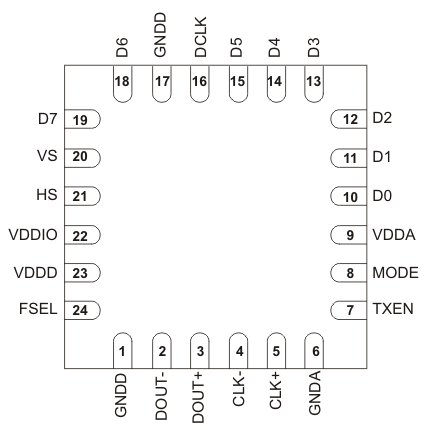
Pin Functions
| PIN | DESCRIPTION | |||
|---|---|---|---|---|
| NO. | NAME | TYPE | ||
| 2, 3, | DOUT+, DOUT– | SubLVDS out | SubLVDS data link CSI-1 compliant (active during normal operation; high-impedance during power down or standby) DOUT is valid on the rising edge of CLK+. | |
| 4, 5, | CLK+, CLK– | SubLVDS clock output (CSI-1 Mode 0 compliant) | ||
| 10, 11, 12, 13, 14, 15, 18, 19 | D0–D7 | CMOS in(1) | Data inputs (8) for pixel data; These inputs are sampled on the falling DCLK edge; inputs incorporate bus hold Note: D[7:0] states are latched into the SN65LVDS315 on the falling DCLK input edge |
|
| 20 | VS | Vertical Sync (also called frame sync); Data input (high active). This input is sampled on every falling DCLK edge Input incorporates bus hold |
||
| 21 | HS | Horizontal Sync (also called line sync); Data input (high active). This input is sampled on every falling DCLK edge Input incorporates bus hold |
||
| 16 | DCLK | Data input Clock; DCLK represents the camera pixel clock. All 8 pixel bits as well as VS and HS are latched into the device on the falling edge of DCLK (falling edge clocking) Input incorporates bus hold |
||
| 7 | TXEN | CMOS in(2) | Disables the subLVDS Drivers and turns off the PLL putting device in Shutdown mode | |
| 1 – Transmitter enabled | ||||
| 0 – Transmitter disabled (shutdown) | ||||
| Note: TXEN input incorporates glitch-suppression logic to avoid device malfunction on short input spikes. It is necessary to pull TXEN high for longer than 10 μs to enable the transmitter. It is necessary to pull the TXEN input low for longer than 10 μs to disable the transmitter. At power up, the transmitter is enabled immediately if TXEN = 1 and disabled if TXEN = 0. Do not leave TXEN floating. |
||||
| 24 | FSEL | Frequency Select | ||
| FSEL=0: DCLK input frequencies from 3.5 MHz to 13 MHz are supported FSEL=1: DCLK input frequencies from 7.0 MHz to 27 MHz are supported Do not leave FSEL floating. |
||||
| 8 | MODE | The mode pin enables line counting to generate proper EOF signalling in case VS and HS do not reset during the same DCLK cycle (0-line counter disable; 1-counter enabled). The impact of the MODE pin setting is described in detail in the VS and HS Timing to Generate the Correct Control Signals section. If you are unsure about the proper setting of the MODE input, it is recommended to set MODE=high. Do not leave the MODE input floating. | ||
| 22 | VDDIO | Power Supply(3) | IO Supply Voltage for inputs D[0:7], HS, VS, and DCLK, (1.8 V up to 3.3 V) | |
| 23 | VDDD | Digital supply voltage (1.8 V only) | ||
| 17 | GNDD | Supply Ground for VDDIO and VDDD | ||
| 9 | VDDA | PLL and SubLVDS I/O supply voltage (1.8 V only) | ||
| 6 | GNDA | PLL and SubLVDS Ground | ||
(1) These inputs are referenced to the VDDIO supply rail and support a voltage range of 1.65 V to 3.6 V
(2) These inputs can tolerate an input voltage up to 3.6 V while the actual input threshold from logic low to logic high is at 0.9 V nominal; This allows driving these inputs from a 1.8 V or 3.3 V GPIO independent of the camera supply voltage.
(3) In a multilayer PCB, it is recommended to keep one common GND layer underneath the device and connect all ground terminals directly to this plane.