JAJSCW3A December 2016 – February 2020 SN65MLVD206B
PRODUCTION DATA.
- 1 特長
- 2 アプリケーション
- 3 概要
- 4 改訂履歴
- 5 概要(続き)
- 6 Pin Configuration and Functions
-
7 Specifications
- Table 1. Absolute Maximum Ratings
- Table 2. ESD Ratings
- Table 3. Recommended Operating Conditions
- Table 4. Thermal Information
- Table 5. Electrical Characteristics
- Table 6. Electrical Characteristics – Driver
- Table 7. Electrical Characteristics – Receiver
- Table 8. Electrical Characteristics – BUS Input and Output
- Table 9. Switching Characteristics – Driver
- Table 10. Switching Characteristics – Receiver
- 7.1 Typical Characteristics
- 8 Parameter Measurement Information
- 9 Detailed Description
-
10Application and Implementation
- 10.1 Application Information
- 10.2
Typical Application
- 10.2.1 Multipoint Communications
- 10.2.2 Design Requirements
- 10.2.3
Detailed Design Procedure
- 10.2.3.1 Supply Voltage
- 10.2.3.2 Supply Bypass Capacitance
- 10.2.3.3 Driver Input Voltage
- 10.2.3.4 Driver Output Voltage
- 10.2.3.5 Termination Resistors
- 10.2.3.6 Receiver Input Signal
- 10.2.3.7 Receiver Input Threshold (Failsafe)
- 10.2.3.8 Receiver Output Signal
- 10.2.3.9 Interconnecting Media
- 10.2.3.10 PCB Transmission Lines
- 10.2.4 Application Curves
- 11Power Supply Recommendations
- 12Layout
- 13デバイスおよびドキュメントのサポート
- 14メカニカル、パッケージ、および注文情報
12.1.3 Recommended Stack Layout
Following the choice of dielectrics and design specifications, you must decide how many levels to use in the stack. To reduce the TTL/CMOS to M-LVDS crosstalk, it is a good practice to have at least two separate signal planes as shown in Figure 24.
 Figure 24. Four-Layer PCB Board
 NOTE
The separation between layers 2 and 3 should be 127 μm (0.005 in). By keeping the power and ground planes tightly coupled, the increased capacitance acts as a bypass for transients.
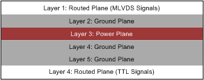
One of the most common stack configurations is the six-layer board, as shown in Figure 25.
 Figure 25. Six-Layer PCB Board
 In this particular configuration, it is possible to isolate each signal layer from the power plane by at least one ground plane. The result is improved signal integrity; however, fabrication is more expensive. Using the 6-layer board is preferable, because it offers the layout designer more flexibility in varying the distance between signal layers and referenced planes, in addition to ensuring reference to a ground plane for signal layers 1 and 6.