JAJSC93E June 2016 – December 2017 TAS2560
PRODUCTION DATA.
- 1 特長
- 2 アプリケーション
- 3 概要
- 4 改訂履歴
- 5 Device Comparison Table
- 6 Pin Configuration and Functions
-
7 Specifications
- 7.1 Absolute Maximum Ratings
- 7.2 ESD Ratings
- 7.3 Recommended Operating Conditions
- 7.4 Thermal Information
- 7.5 Electrical Characteristics
- 7.6 I2C Timing Requirements
- 7.7 I2S/LJF/RJF Timing in Master Mode
- 7.8 I2S/LJF/RJF Timing in Slave Mode
- 7.9 DSP Timing in Master Mode
- 7.10 DSP Timing in Slave Mode
- 7.11 PDM Timing
- 7.12 Typical Characteristics
- 8 Parameter Measurement Information
-
9 Detailed Description
- 9.1 Overview
- 9.2 Functional Block Diagram
- 9.3
Feature Description
- 9.3.1 General I2C Operation
- 9.3.2 Single-Byte and Multiple-Byte Transfers
- 9.3.3 Single-Byte Write
- 9.3.4 Multiple-Byte Write and Incremental Multiple-Byte Write
- 9.3.5 Single-Byte Read
- 9.3.6 Multiple-Byte Read
- 9.3.7 PLL
- 9.3.8 Clock Distribution
- 9.3.9 Clock Error Detection
- 9.3.10 Class-D Edge Rate Control
- 9.3.11 IV Sense
- 9.3.12 Boost Control
- 9.3.13 Thermal Fold-back
- 9.3.14 Battery Guard AGC
- 9.3.15 Configurable Boost Current Limit (ILIM)
- 9.3.16 Fault Protection
- 9.3.17 Spread Spectrum vs Synchronized
- 9.3.18 IRQs and Flags
- 9.3.19 CRC checksum for I2C
- 9.3.20 PurePath Console 3 Software TAS2560 Application
- 9.4 Device Functional Modes
- 9.5 Operational Modes
- 9.6 Programming
- 9.7
Register Map
- 9.7.1 Register Map Summary
- 9.7.2 PAGE (book=0x00 page=0x00 address=0x00) [reset=0h]
- 9.7.3 RESET (book=0x00 page=0x00 address=0x01) [reset=0h]
- 9.7.4 MODE (book=0x00 page=0x00 address=0x02) [reset=1h]
- 9.7.5 SPK_CTRL (book=0x00 page=0x00 address=0x04) [reset=5Fh]
- 9.7.6 PWR_CTRL_2 (book=0x00 page=0x00 address=0x05) [reset=0h]
- 9.7.7 PWR_CTRL_1 (book=0x00 page=0x00 address=0x07) [reset=0h]
- 9.7.8 RAMP_CTRL (book=0x00 page=0x00 address=0x08) [reset=1h]
- 9.7.9 EDGE_ISNS_BOOST (book=0x00 page=0x00 address=0x09) [reset=83h]
- 9.7.10 PLL_CLKIN (book=0x00 page=0x00 address=0x0F) [reset=41h]
- 9.7.11 PLL_JVAL (book=0x00 page=0x00 address=0x10) [reset=4h]
- 9.7.12 PLL_DVAL_1 (book=0x00 page=0x00 address=0x11) [reset=0h]
- 9.7.13 PLL_DVAL_2 (book=0x00 page=0x00 address=0x12) [reset=0h]
- 9.7.14 ASI_FORMAT (book=0x00 page=0x00 address=0x14) [reset=2h]
- 9.7.15 ASI_CHANNEL (book=0x00 page=0x00 address=0x15) [reset=0h]
- 9.7.16 ASI_OFFSET_1 (book=0x00 page=0x00 address=0x16) [reset=0h]
- 9.7.17 ASI_OFFSET_2 (book=0x00 page=0x00 address=0x17) [reset=0h]
- 9.7.18 ASI_CFG_1 (book=0x00 page=0x00 address=0x18) [reset=0h]
- 9.7.19 ASI_DIV_SRC (book=0x00 page=0x00 address=0x19) [reset=0h]
- 9.7.20 ASI_BDIV (book=0x00 page=0x00 address=0x1A) [reset=1h]
- 9.7.21 ASI_WDIV (book=0x00 page=0x00 address=0x1B) [reset=40h]
- 9.7.22 PDM_CFG (book=0x00 page=0x00 address=0x1C) [reset=0h]
- 9.7.23 PDM_DIV (book=0x00 page=0x00 address=0x1D) [reset=8h]
- 9.7.24 DSD_DIV (book=0x00 page=0x00 address=0x1E) [reset=8h]
- 9.7.25 CLK_ERR_1 (book=0x00 page=0x00 address=0x21) [reset=3h]
- 9.7.26 CLK_ERR_2 (book=0x00 page=0x00 address=0x22) [reset=3Fh]
- 9.7.27 IRQ_PIN_CFG (book=0x00 page=0x00 address=0x23) [reset=21h]
- 9.7.28 INT_CFG_1 (book=0x00 page=0x00 address=0x24) [reset=0h]
- 9.7.29 INT_CFG_2 (book=0x00 page=0x00 address=0x25) [reset=0h]
- 9.7.30 INT_DET_1 (book=0x00 page=0x00 address=0x26) [reset=0h]
- 9.7.31 INT_DET_2 (book=0x00 page=0x00 address=0x27) [reset=0h]
- 9.7.32 STATUS_POWER (book=0x00 page=0x00 address=0x2A) [reset=0h]
- 9.7.33 SAR_VBAT_MSB (book=0x00 page=0x00 address=0x2D) [reset=C0h]
- 9.7.34 SAR_VBAT_LSB (book=0x00 page=0x00 address=0x2E) [reset=0h]
- 9.7.35 DIE_TEMP_SENSOR (book=0x00 page=0x00 address=0x31) [reset=0h]
- 9.7.36 LOW_PWR_MODE (book=0x00 page=0x00 address=0x35) [reset=0h]
- 9.7.37 PCM_RATE (book=0x00 page=0x00 address=0x36) [reset=32h]
- 9.7.38 CLOCK_ERR_CFG_1 (book=0x00 page=0x00 address=0x4F) [reset=0h]
- 9.7.39 CLOCK_ERR_CFG_2 (book=0x00 page=0x00 address=0x50) [reset=11h]
- 9.7.40 PROTECTION_CFG_1 (book=0x00 page=0x00 address=0x58) [reset=3h]
- 9.7.41 CRC_CHECKSUM (book=0x00 page=0x00 address=0x7E) [reset=0h]
- 9.7.42 BOOK (book=0x00 page=0x00 address=0x7F) [reset=0h]
- 10Application and Implementation
- 11Power Supply Recommendations
- 12Layout
- 13デバイスおよびドキュメントのサポート
- 14メカニカル、パッケージ、および注文情報
パッケージ・オプション
デバイスごとのパッケージ図は、PDF版データシートをご参照ください。
メカニカル・データ(パッケージ|ピン)
- YFF|30
サーマルパッド・メカニカル・データ
発注情報
7 Specifications
7.1 Absolute Maximum Ratings
over operating free-air temperature range, TA = 25°C (unless otherwise noted)| MIN | MAX | UNIT | ||
|---|---|---|---|---|
| Battery voltage | VBAT | –0.3 | 6 | V |
| Analog supply voltage | VDD | –0.3 | 2 | V |
| I/O supply voltage | IOVDD | –0.3 | 3.9 | V |
| Boost | VBST | –0.3 | 9.2 | V |
| Switching | SW | –0.7 | VBST + 1.8(1) | V |
| Regulator voltage | VREG | –0.3 | VBST + 5 | V |
| Digital input voltage | –0.3 | IOVDD + 0.3 | V | |
| Output continuous total power dissipation | See Thermal Information | |||
| Storage temperature, Tstg | –65 | 150 | °C | |
7.2 ESD Ratings
| VALUE | UNIT | |||
|---|---|---|---|---|
| V(ESD) | Electrostatic discharge | Human-body model (HBM), per ANSI/ESDA/JEDEC JS-001(1) | ±2500 | V |
| Charged-device model (CDM), per JEDEC specification JESD22-C101(2) | ±1500 | |||
(1) JEDEC document JEP155 states that 500-V HBM allows safe manufacturing with a standard ESD control process.
(2) JEDEC document JEP157 states that 250-V CDM allows safe manufacturing with a standard ESD control process.
7.3 Recommended Operating Conditions
over operating free-air temperature range, TA = 25°C (unless otherwise noted)| MIN | NOM | MAX | UNIT | |||
|---|---|---|---|---|---|---|
| Battery voltage | VBAT | 2.9(1) | 3.6 | 5.5 | V | |
| Analog supply voltage | VDD | 1.65 | 1.8 | 1.95 | V | |
| I/O supply voltage 1.8V | IOVDD | 1.62 | 1.8 | 1.98 | V | |
| I/O supply voltage 3.3V | IOVDD | 3 | 3.3 | 3.6 | V | |
| TA | Operating free-air temperature | –40 | 85 | °C | ||
| TJ | Operating junction temperature | –40 | 150 | °C | ||
(1) Device is functional down to 2.7 V. See Battery Guard AGC
7.4 Thermal Information
| THERMAL METRIC(1) | TAS2560 | UNIT | |
|---|---|---|---|
| 30 PINS | |||
| RθJA | Junction-to-ambient thermal resistance | 56.8 | °C/W |
| RθJC(top) | Junction-to-case (top) thermal resistance | 0.2 | |
| RθJB | Junction-to-board thermal resistance | 8.1 | |
| ψJT | Junction-to-top characterization parameter | 1.2 | |
| ψJB | Junction-to-board characterization parameter | 8.1 | |
| RθJC(bot) | Junction-to-case (bottom) thermal resistance | n/a | |
(1) For more information about traditional and new thermal metrics, see the Semiconductor and IC Package Thermal Metrics application report.
7.5 Electrical Characteristics
VBAT = 3.6 V, VDD = IOVDD = 1.8 V, RESETZ = IOVDD, Gain = 16.4 dB, ERC = 14 ns, Boost Inductor = 2.2 µH, RL = 8 Ω + 33 µH, 1-kHz input frequency, 48-kHz sample rate for digital input, Class-H Boost Enabled, TA= 25°C, ILIM = 3 A (unless otherwise noted)| PARAMETER | TEST CONDITIONS | MIN | TYP | MAX | UNIT | |
|---|---|---|---|---|---|---|
| BOOST CONVERTER | ||||||
| Boost output voltage | Average voltage (w/o including ripple). | 8.5 | V | |||
| Boost converter switching frequency | 1.77 | MHz | ||||
| Boost converter current limit | 3 | A | ||||
| Boost converter max in-rush current | High Efficiency Mode: Max inductor in-rush and startup current after enable | 4 | A | |||
| Normal Efficiency Mode: Max inductor in-rush and startup current after enable | 1.5 | |||||
| CLASS-D CHANNEL | ||||||
| Output voltage for full-scale digital input | 6.67 | VRMS | ||||
| Load resistance (Load spec resistance) | 3.6 | 8 | Ω | |||
| Class-D frequency | Avg frequency in spread-spectrum mode | 384 | kHz | |||
| Fixed Frequency | 44.1 × 8 | 48 × 8 | ||||
| Class-D + boost efficiency | POUT = 3.5 W (sinewave) ROM Mode 1 | 81% | ||||
| POUT = 0.44 W (sinewave) ROM Mode 1 | 87% | |||||
| Class-D output current limit (Short circuit protection) | VBOOST = 8.5 V, OUT– shorted to VBAT, VBOOST, GND | 4 | A | |||
| Class-D output offset voltage in digital input mode | –2.5 | 2.5 | mV | |||
| Programmable channel gain accuracy | ±0.5 | dB | ||||
| Mute attenuation | Device in shutdown or device in normal operation and MUTED | 146 | dB | |||
| VBAT Power Supply Rejection Ratio (PSRR) | Ripple of 200 mVpp at 217 Hz | 110 | dB | |||
| AVDD Power Supply Rejection Ratio (PSRR) | Ripple of 200 mVpp at 217 Hz | 98 | dB | |||
| THD+N | 1 kHz, POUT = 0.1 W | 0.0085% | ||||
| 1 kHz, Po = 0.5 W | 0.0046% | |||||
| 1 kHz, Po = 1 W | 0.0035% | |||||
| 1 kHz, Po = 3 W | 0.0043% | |||||
| Output integrated noise (20 Hz to 20 kHz) - 8 Ω | A-wt Filter, DAC modulator switching | 16.2 | µV | |||
| Signal-to-noise ratio | Referenced to 1% THD+N at output, a-weighted | 110.6 | dB | |||
| Max output power, 3-A current limit | THD+N = 1%, 8-Ω Load | 3.7 | W | |||
| THD+N = 1%, 6-Ω Load | 4.5 | |||||
| THD+N = 1%, 4-Ω Load | 5 | |||||
| Startup pop | Digital input, a-weighted output | 5 | mV | |||
| Output impedance in shutdown | RESETZ = 0 V | 10.4 | kΩ | |||
| Startup time | Time taken from end of configuring device to speaker output signal in I2C mode with 48ksps input | 8 | mS | |||
| Shutdown time | Measured from time when device is programmed in software shutdown mode | 100 | µS | |||
| CURRENT SENSE | ||||||
| Current sense full scale | Peak current which will give full scale digital output 8-Ω load | 1.25 | APEAK | |||
| Peak current which will give full scale digital output 8-Ω load PDM | 4.022 | |||||
| Peak current which will give full scale digital output 6-Ω load | 1.5 | |||||
| Peak current which will give full scale digital output 4-Ω load | 1.75 | |||||
| Current sense accuracy | IOUT = 354 mARMS (1 W) | 1.7% | ||||
| Current sense gain drift over temperature | –40°C to 85°C | 4% | ||||
| Current sense gain linearity | From 15 mW to 3.5 W for fin=1 kHz | 1.5% | ||||
| THD+N | Distortion + Noise | POUT = 3 W (Load = 8 Ω + 33 µH) | 0.196% | |||
| POUT = 3 W (Load = 4 Ω + 33 µH) | 0.132% | |||||
| SNR | 20 Hz to 20 kHz, A-wt | –68 | db | |||
| VOLTAGE SENSE | ||||||
| Voltage sense full scale | Peak voltage which will give full scale digital output(1) | 9.353 | VPEAK | |||
| Peak voltage which will give full scale digital output in PDM | 16.65 | |||||
| Voltage sense accuracy | VOUT = 2.83 Vrms (1 W) | 1% | ||||
| Voltage sense gain drift over temperature | –40°C to 85°C | 1.2% | ||||
| Voltage sense gain linearity | From 15 mW to 3.5 W for fin = 1 kHz | 1% | ||||
| INTERFACE | ||||||
| Voltage and current sense data rate | TDM/I2S | 48 | kHz | |||
| Voltage and current sense ADC OSR | TDM/I2S | 64 | OSR | |||
| FMCLK | MCLK frequency | 0.512 | 49.15 | MHz | ||
| POWER CONSUMPTION | ||||||
| Power consumption with digital input and IV-sense disabled. Idle channel condition | From VBAT, no signal | 3.2 | mA | |||
| From VDD, no signal | 9.5 | mA | ||||
| Power consumption with digital input and IV-sense enabled. | From VBAT, no signal | 3.2 | mA | |||
| From VDD, no signal | 10.6 | mA | ||||
| Power consumption in hardware shutdown | From VBAT, RESETZ = 0 | 0.1 | µA | |||
| From VDD, RESETZ = 0 | 1.2 | µA | ||||
| Power consumption in software shutdown. See Low Power Sleep | From VBAT | 0.1 | µA | |||
| From VDD | 9.8 | µA | ||||
| DIGITAL INPUT / OUTPUT | ||||||
| VIH | High-level digital input voltage | All digital pins except SDA and SCL, IOVDD = 1.8-V operation | 0.65 × IOVDD | V | ||
| VIL | Low-level digital input voltage | 0.35 × IOVDD | V | |||
| VIH | High-level digital input voltage | All digital pins except SDA and SCL, IOVDD = 3.3-V operation | 2 | V | ||
| VIL | Low-level digital input voltage | 0.45 | V | |||
| VOH | High-level digital output voltage | All digital pins except SDA and SCL, IOVDD = 1.8-V operation For IOL = 2 mA and IOH = –2 mA | IOVDD – 0.45 | V | ||
| VOL | Low-level digital output voltage | 0.45 | V | |||
| VOH | High-level digital output voltage | All digital pins except SDA and SCL, IOVDD = 3.3-V operation For IOL = 2 mA and IOH = –2 mA | 2.4 | V | ||
| VOL | Low-level digital output voltage | 0.4 | V | |||
| IIH | High-level digital input leakage current | Input = IOVDD | –5 | 0.1 | 5 | µA |
| IIL | Low-level digital input leakage current | Input = Ground | –5 | 0.1 | 5 | µA |
| MISCELLANEOUS | ||||||
| TTRIP | Thermal Trip Point | 135 | °C | |||
(1) Voltage Sense Fullscale = 1.176 Vrms × 10(DAC_GAIN/20)
7.6 I2C Timing Requirements
For I2C interface signals over recommended operating conditions (unless otherwise noted).(1)| PARAMETER | TEST CONDITION | Standard-Mode | Fast-Mode | UNITS | |||||
|---|---|---|---|---|---|---|---|---|---|
| MIN | TYP | MAX | MIN | TYP | MAX | ||||
| fSCL | SCL clock frequency | 0 | 100 | 0 | 400 | kHz | |||
| tHD;STA | Hold time (repeated) START condition. After this period, the first clock pulse is generated. | 4 | 0.6 | μs | |||||
| tLOW | LOW period of the SCL clock | 4.7 | 1.3 | μs | |||||
| tHIGH | HIGH period of the SCL clock | 4 | 0.6 | μs | |||||
| tSU;STA | Setup time for a repeated START condition | 4.7 | 0.6 | μs | |||||
| tHD;DAT | Data hold time: For I2C bus devices | 0 | 3.45 | 0 | 0.9 | μs | |||
| tSU;DAT | Data set-up time | 250 | 100 | ns | |||||
| tr | SDA and SCL Rise Time | 1000 | 20 + 0.1 × Cb | 300 | ns | ||||
| tf | SDA and SCL Fall Time | 300 | 20 + 0.1 × Cb | 300 | ns | ||||
| tSU;STO | Set-up time for STOP condition | 4 | 0.6 | μs | |||||
| tBUF | Bus free time between a STOP and START condition | 4.7 | 1.3 | μs | |||||
| Cb | Capacitive load for each bus line | 400 | 400 | pF | |||||
(1) All timing specifications are specified by design but not tested at final test.
7.7 I2S/LJF/RJF Timing in Master Mode
All specifications at TA = –40°C to 85°C, IOVDD data sheet limits, VIL and VIH applied, VOL and VOH measured at datasheet limits, lumped capacitive load of 20 pF on output pins unless otherwise noted.(1)| SYMBOL | PARAMETER | CONDITIONS | IOVDD = 1.8 V | IOVDD = 3.3 V | UNIT | ||
|---|---|---|---|---|---|---|---|
| MIN | MAX | MIN | MAX | ||||
| td(WS) | BCLK to WCLK delay | 50% of BCLK to 50% of WCLK | 35 | 25 | ns | ||
| td(DO-WS) | WCLK to DOUT delay (For LJF Mode only) | 50% of WCLK to 50% of DOUT | 35 | 25 | ns | ||
| td(DO-BCLK) | BCLK to DOUT delay | 50% of BCLK to 50% of DOUT | 35 | 25 | ns | ||
| ts(DI) | DIN setup | 8 | 8 | ns | |||
| th(DI) | DIN hold | 8 | 8 | ns | |||
| tr | Rise time | 10%-90% Rise Time | 8 | 4 | ns | ||
| tf | Fall time | 90%-10% Fall Time | 8 | 4 | ns | ||
(1) All timing specifications are measured at characterization but not tested at final test.
7.8 I2S/LJF/RJF Timing in Slave Mode
All specifications at TA = –40°C to 85°C, IOVDD data sheet limits, VIL and VIH applied, VOL and VOH measured at datasheet limits, lumped capacitive load of 20 pF on output pins unless otherwise noted.(1)| SYMBOL | PARAMETER | CONDITIONS | IOVDD = 1.8 V | IOVDD = 3.3 V | UNIT | ||
|---|---|---|---|---|---|---|---|
| MIN | MAX | MIN | MAX | ||||
| tH(BCLK) | BCLK high period | 40 | 30 | ns | |||
| tL(BCLK) | BCLK low period | 40 | 30 | ns | |||
| ts(WS) | (WS) | 8 | 8 | ns | |||
| th(WS) | WCLK hold | 8 | 8 | ns | |||
| td(DO-WS) | WCLK to DOUT delay (For LJF Mode only) | 50% of WCLK to 50% of DOUT | 35 | 25 | ns | ||
| td(DO-BCLK) | BCLK to DOUT delay | 50% of BCLK to 50% of DOUT | 35 | 25 | ns | ||
| ts(DI) | DIN setup | 8 | 8 | ns | |||
| th(DI) | DIN hold | 8 | 8 | ns | |||
| tr | Rise time | 10%-90% Rise Time | 8 | 4 | ns | ||
| tf | Fall time | 90%-10% Fall Time | 8 | 4 | ns | ||
(1) All timing specifications are measured at characterization but not tested at final test.
7.9 DSP Timing in Master Mode
All specifications at TA = –40°C to 85°C, IOVDD data sheet limits, VIL and VIH applied, VOL and VOH measured at datasheet limits, lumped capacitive load of 20 pF on output pins unless otherwise noted.(1)| SYMBOL | PARAMETER | CONDITIONS | IOVDD = 1.8 V | IOVDD = 3.3 V | UNIT | ||
|---|---|---|---|---|---|---|---|
| MIN | MAX | MIN | MAX | ||||
| td(WS) | BCLK to WCLK delay | 50% of BCLK to 50% of WCLK | 35 | 25 | ns | ||
| td(DO-BCLK) | BCLK to DOUT delay | 50% of BLCK to 50% of DOUT | 35 | 25 | ns | ||
| ts(DI) | DIN setup | 8 | 8 | ns | |||
| th(DI) | DIN hold | 8 | 8 | ns | |||
| tr | Rise time | 10%-90% Rise Time | 8 | 4 | ns | ||
| tf | Fall time | 90%-10% Fall Time | 8 | 4 | ns | ||
(1) All timing specifications are measured at characterization but not tested at final test.
7.10 DSP Timing in Slave Mode
All specifications at TA = –40°C to 85°C, IOVDD data sheet limits, VIL and VIH applied, VOL and VOH measured at datasheet limits, lumped capacitive load of 20 pF on output pins unless otherwise noted.(1)| SYMBOL | PARAMETER | CONDITIONS | IOVDD=1.8V | IOVDD=3.3V | UNIT | ||
|---|---|---|---|---|---|---|---|
| MIN | MAX | MIN | MAX | ||||
| tH(BCLK) | BCLK high period | 40 | 30 | ns | |||
| tL(BCLK) | BCLK low period | 40 | 30 | ns | |||
| ts(WS) | WCLK seutp | 8 | 8 | ns | |||
| th(WS) | WCLK hold | 8 | 8 | ns | |||
| td(DO-BCLK) | BCLK to DOUT delay (For LJF Mode only) | 50% BCLK to 50% DOUT | 35 | 25 | ns | ||
| ts(DI) | DIN setup | 8 | 8 | ns | |||
| th(DI) | DIN hold | 8 | 8 | ns | |||
| tr | Rise time | 10%-90% Rise Time | 8 | 4 | ns | ||
| tf | Fall time | 90%-10% Fall Time | 8 | 4 | ns | ||
(1) All timing specifications are measured at characterization but not tested at final test.
7.11 PDM Timing
All specifications at TA = –40°C to 85°C, IOVDD data sheet limits, VIL and VIH applied, VOL and VOH measured at datasheet limits, lumped capacitive load of 20 pF on output pins unless otherwise noted.(1)| PARAMETER | CONDITIONS | IOVDD = 1.8 V | IOVDD = 3.3 V | UNIT | |||
|---|---|---|---|---|---|---|---|
| MIN | MAX | MIN | MAX | ||||
| ts | DIN setup | 20 | 20 | ns | |||
| th | DIN hold | 3 | 3 | ns | |||
| tr | Rise time | 10%-90% Rise Time | 8 | 4 | ns | ||
| tf | Fall time | 90%-10% Fall Time | 8 | 4 | ns | ||
(1) All timing specifications are measured at characterization but not tested at final test.
 Figure 1. I2C Timing
 Figure 2. I2S/LJF/RJF Timing in Master Mode
 Figure 3. I2S/LJF/RJF Timing in Slave Mode
 Figure 4. DSP Timing in Master Mode
 Figure 5. DSP Timing in Slave Mode
 Figure 6. PDM Timing
7.12 Typical Characteristics
VBAT = 3.6 V, VDD = IOVDD = 1.8 V, RESETZ = IOVDD, RL = 8 Ω + 33 µH, I2S digital input, Mode 2 (unless otherwise noted).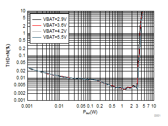
| 8 Ω + 33 µH | Freq = 1 kHz |
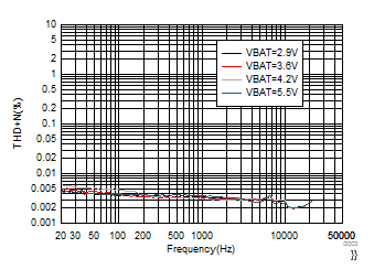
| 8 Ω + 33 µH | POUT = 1 W |
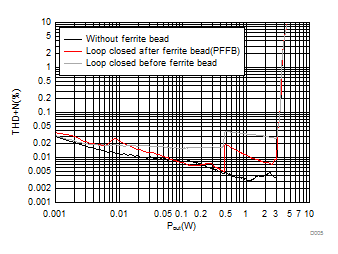
| 8 Ω + 33 µH | Freq = 1 kHz |
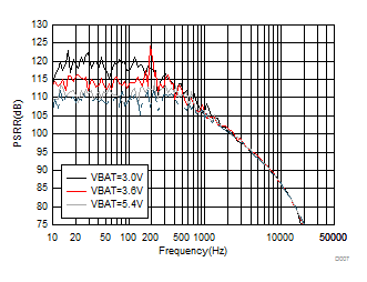
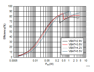
| 8 Ω + 33 µH | SSM Mode | |||

| 8 Ω + 33 µH | SSM Mode | |||
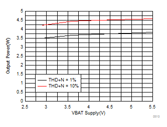
| 8 Ω+ 33 µH |
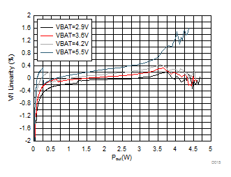
| 8 Ω + 33 µH |
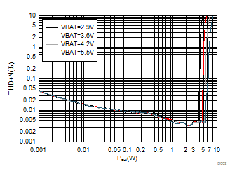
| 4 Ω + 16 µH | Freq = 1 kHz |
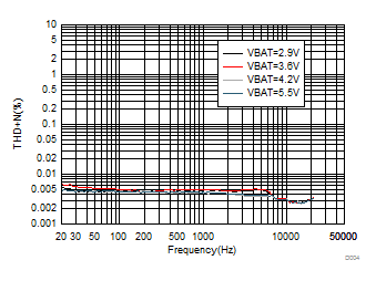
| 4 Ω + 16 µH | POUT = 1 W |
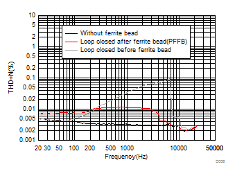
| 8 Ω + 33 µH | POUT = 1 W |
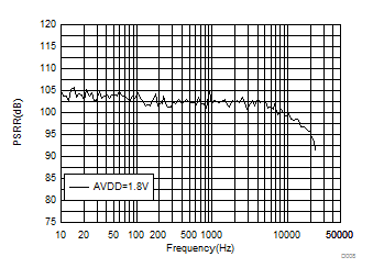
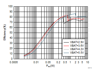
| 4 Ω + 16 µH | SSM Mode | |||
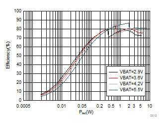
| 4 Ω + 16 µH | SSM Mode | |||
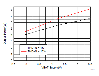
| 4 Ω+ 16 µH |
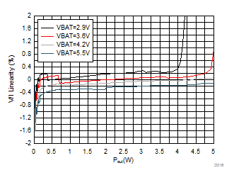
| 4 Ω+ 16µH |