SLOS358C September 2011 – April 2020 THS4531
PRODUCTION DATA.
- 1 Features
- 2 Applications
- 3 Description
- 4 Revision History
- 5 Packaging and Ordering Information
- 6 Electrical Specifications
- 7 Device Information
- 8 Table of Graphs
- 9 Typical Characteristics: VS = 2.7 V
- 10Typical Characteristics: VS = 5 V
-
11Application Information
- 11.1 Typical Characteristics Test Circuits
- 11.2
Application Circuits
- 11.2.1 Differential Input to Differential Output Amplifier
- 11.2.2 Single-Ended Input to Differential Output Amplifier
- 11.2.3 Differential Input to Single-Ended Output Amplifier
- 11.2.4 Input Common-Mode Voltage Range
- 11.2.5 Setting the Output Common-Mode Voltage
- 11.2.6 Single-Supply Operation
- 11.2.7 Low Power Applications and the Effects of Resistor Values on Bandwidth
- 11.2.8 Driving Capacitive Loads
- 11.2.9 Audio Performance
- 11.2.10 Audio On and Off Pop Performance
- 11.3 Audio ADC Driver Performance: THS4531 AND PCM4204 Combined Performance
- 11.4 SAR ADC Performance
- 11.5 EVM and Layout Recommendations
- 12Device and Documentation Support
- 13Mechanical, Packaging, and Orderable Information
パッケージ・オプション
メカニカル・データ(パッケージ|ピン)
サーマルパッド・メカニカル・データ
発注情報
11.4.2 THS4531 and ADS7945 Combined Performance
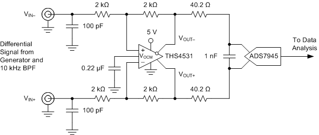
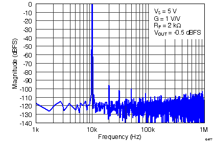
To show achievable performance with a high performance SAR ADC, the THS4531 is tested as the drive amplifier for the ADS7945. The ADS7945 is a 14-bit, SAR ADC that offers excellent AC and DC performance, with low power and small size. The circuit shown in Figure 90 is used to test the performance. Data was taken using the ADS7945 at 2MSPS with input frequency of 10 kHz and signal level 0.5 dB below full scale. The FFT plot of the spectral performance is in Figure 91. A summary of the FFT analysis results are in Table 7 along with ADS7945 typical data sheet performance at fS = 2 MSPS. Please refer to its data sheet for more information.
The standard ADS7945 EVM and THS4531 EVM are modified to implement the schematic in Figure 90 and used to test the performance of the THS4531 as a drive amplifier. With single supply +5 V supply the output common-mode of the THS4531 defaults to +2.5 V as required at the input of the ADS7945 so the VOCM input of the THS4531 simply bypassed to GND with 0.22 µF capacitor. The summary of results of the FFT analysis versus typical data sheet performance shown in Table 7 show the THS4531 will make an excellent drive amplifier for this ADC.
 Figure 90. THS4531 and ADS7945 Test Circuit
  Figure 91. THS4531 and ADS7945 Test Circuit
 Table 7. 10 kHz FFT Analysis Summary
| CONFIGURATION | TONE | SIGNAL | SNR | THD | SFDR |
|---|---|---|---|---|---|
| THS4531 + ADS7945 | 10 kHz | -0.5 dBFS | 83 dBc | -93 dBc | 96 dBc |
| ADS7945 Data sheet (typical) | 10 kHz | -0.5 dBFS | 84 dBc | -92 dBc | 94 dBc |