SLOS358C September 2011 – April 2020 THS4531
PRODUCTION DATA.
- 1 Features
- 2 Applications
- 3 Description
- 4 Revision History
- 5 Packaging and Ordering Information
- 6 Electrical Specifications
- 7 Device Information
- 8 Table of Graphs
- 9 Typical Characteristics: VS = 2.7 V
- 10Typical Characteristics: VS = 5 V
-
11Application Information
- 11.1 Typical Characteristics Test Circuits
- 11.2
Application Circuits
- 11.2.1 Differential Input to Differential Output Amplifier
- 11.2.2 Single-Ended Input to Differential Output Amplifier
- 11.2.3 Differential Input to Single-Ended Output Amplifier
- 11.2.4 Input Common-Mode Voltage Range
- 11.2.5 Setting the Output Common-Mode Voltage
- 11.2.6 Single-Supply Operation
- 11.2.7 Low Power Applications and the Effects of Resistor Values on Bandwidth
- 11.2.8 Driving Capacitive Loads
- 11.2.9 Audio Performance
- 11.2.10 Audio On and Off Pop Performance
- 11.3 Audio ADC Driver Performance: THS4531 AND PCM4204 Combined Performance
- 11.4 SAR ADC Performance
- 11.5 EVM and Layout Recommendations
- 12Device and Documentation Support
- 13Mechanical, Packaging, and Orderable Information
パッケージ・オプション
メカニカル・データ(パッケージ|ピン)
サーマルパッド・メカニカル・データ
発注情報
11.1.5 VOCM Input
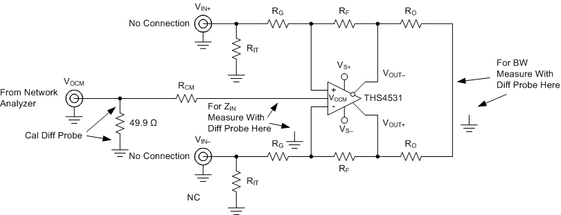
The circuit shown in Figure 71 is used to measure the transient response, frequency response and input impedance of the VOCM input. For these tests, the cal point is across the 49.9 Ω VOCM termination resistor. Transient response and frequency response are measured with RCM = 0 Ω and using a high impedance differential probe at the summing junction of the two RO resistors, with respect to ground. The input impedance is measured using a high impedance differential probe at the VOCM pin and the drop across RCM is used to calculate the impedance seen looking into the amplifier’s VOCM input.
 Figure 71. VOCM Input Test Circuit