SLLSEF8C August 2013 – November 2014 TLK111
PRODUCTION DATA.
- 1 Introduction
- 2 Pin Descriptions
-
3 Hardware Configuration
- 3.1 Bootstrap Configuration
- 3.2 Power Supply Configuration
- 3.3 IO Pins Hi-Z State During Reset
- 3.4 Auto-Negotiation
- 3.5 Auto-MDIX
- 3.6 PHY Address
- 3.7 MII Isolate Mode
- 3.8 Software Strapping Mode
- 3.9 LED Interface
- 3.10 Multi-Configurable LED (MLED)
- 3.11 Loopback Functionality
- 3.12 BIST
- 3.13 Cable Diagnostics
- 4 Interfaces
-
5 Architecture
- 5.1 100Base-TX Transmit Path
- 5.2
100Base-TX Receive Path
- 5.2.1 Analog Front End
- 5.2.2 Adaptive Equalizer
- 5.2.3 Baseline Wander Correction
- 5.2.4 NRZI and MLT-3 Decoding
- 5.2.5 Descrambler
- 5.2.6 5B/4B Decoder and Nibble Alignment
- 5.2.7 Timing Loop and Clock Recovery
- 5.2.8 Phase-Locked Loops (PLL)
- 5.2.9 Link Monitor
- 5.2.10 Signal Detect
- 5.2.11 Bad SSD Detection
- 5.3 10Base-T Receive Path
- 5.4 Auto Negotiation
- 5.5 Link Down Functionality
- 5.6 IEEE 1588 Precision Timing Protocol Support
- 6 Reset and Power Down Operation
- 7 Design Guidelines
-
8 Register Block
- 8.1
Register Definition
- 8.1.1 Basic Mode Control Register (BMCR)
- 8.1.2 Basic Mode Status Register (BMSR)
- 8.1.3 PHY Identifier Register 1 (PHYIDR1)
- 8.1.4 PHY Identifier Register 2 (PHYIDR2)
- 8.1.5 Auto-Negotiation Advertisement Register (ANAR)
- 8.1.6 Auto-Negotiation Link Partner Ability Register (ANLPAR) (BASE Page)
- 8.1.7 Auto-Negotiate Expansion Register (ANER)
- 8.1.8 Auto-Negotiate Next Page Transmit Register (ANNPTR)
- 8.1.9 Auto-Negotiation Link Partner Ability Next Page Register (ANLNPTR)
- 8.1.10 Software Strap Control register 1 (SWSCR1)
- 8.1.11 Software Strap Control register 2 (SWSCR2)
- 8.1.12 Software Strap Control Register 3 (SWSCR3)
- 8.1.13 Extended Register Addressing
- 8.1.14 Fast Link Down Status Register
- 8.1.15 PHY Status Register (PHYSTS)
- 8.1.16 PHY Specific Control Register (PHYSCR)
- 8.1.17 MII Interrupt Status Register 1 (MISR1)
- 8.1.18 MII Interrupt Status Register 2 (MISR2)
- 8.1.19 False Carrier Sense Counter Register (FCSCR)
- 8.1.20 Receiver Error Counter Register (RECR)
- 8.1.21 BIST Control Register (BISCR)
- 8.1.22 RMII Control and Status Register (RCSR)
- 8.1.23 LED Control Register (LEDCR)
- 8.1.24 PHY Control Register (PHYCR)
- 8.1.25 10Base-T Status/Control Register (10BTSCR)
- 8.1.26 BIST Control and Status Register 1 (BICSR1)
- 8.1.27 BIST Control and Status Register2 (BICSR2)
- 8.2 Cable Diagnostic Control Register (CDCR)
- 8.3 PHY Reset Control Register (PHYRCR)
- 8.4 Multi LED Control register (MLEDCR)
- 8.5 IEEE1588 Precision Timing Pin Select (PTPPSEL)
- 8.6 IEEE1588 Precision Timing Configuration (PTPCFG)
- 8.7 TX_CLK Phase Shift Register (TXCPSR)
- 8.8 Power Back Off Control Register (PWRBOCR)
- 8.9 Voltage Regulator Control Register (VRCR)
- 8.10
Cable Diagnostic Configuration/Result Registers
- 8.10.1 ALCD Control and Results 1 (ALCDRR1)
- 8.10.2 Cable Diagnostic Specific Control Registers (CDSCR1 - CDSCR4)
- 8.10.3 Cable Diagnostic Location Results Register 1 (CDLRR1)
- 8.10.4 Cable Diagnostic Location Results Register 2 (CDLRR2)
- 8.10.5 Cable Diagnostic Location Results Register 3 (DDLRR3)
- 8.10.6 Cable Diagnostic Location Results Register 4 (CDLRR4)
- 8.10.7 Cable Diagnostic Location Results Register 5 (CDLRR5)
- 8.10.8 Cable Diagnostic Amplitude Results Register 1 (CDARR1)
- 8.10.9 Cable Diagnostic Amplitude Results Register 2 (CDARR2)
- 8.10.10 Cable Diagnostic Amplitude Results Register 3 (CDARR3)
- 8.10.11 Cable Diagnostic Amplitude Results Register 4 (CDARR4)
- 8.10.12 Cable Diagnostic Amplitude Results Register 5 (CDARR5)
- 8.10.13 Cable Diagnostic General Results Register (CDGRR)
- 8.10.14 ALCD Control and Results 2 (ALCDRR2)
- 8.10.15 ALCD Control and Results 3 (ALCDRR3)
- 8.1
Register Definition
-
9 Electrical Specifications
- 9.1 Absolute Maximum Ratings
- 9.2 Handling Ratings
- 9.3 Recommended Operating ConditionsRedundant row "Power dissipation 200 mW"
- 9.4 48-Pin Industrial Device Thermal Characteristics
- 9.5 48-Pin Extended Temperature (125°C) Device Thermal Characteristics
- 9.6 DC Characteristics, VDD_IO DC Characteristics, SD_IN
- 9.7 DC Characteristics
- 9.8 Power Supply Characteristics
- 9.9
AC Specifications
- 9.9.1 Power Up Timing
- 9.9.2 Reset Timing
- 9.9.3 MII Serial Management Timing
- 9.9.4 100Mb/s MII Transmit Timing
- 9.9.5 100Mb/s MII Receive Timing
- 9.9.6 100Base-TX Transmit Packet Latency Timing
- 9.9.7 100Base-TX Transmit Packet Deassertion Timing
- 9.9.8 100Base-TX Transmit Timing (tR/F and Jitter)
- 9.9.9 100Base-TX Receive Packet Latency Timing
- 9.9.10 100Base-TX Receive Packet Deassertion Timing
- 9.9.11 10Mbs MII Transmit Timing
- 9.9.12 10Mb/s MII Receive Timing
- 9.9.13 10Base-T Transmit Timing (Start of Packet)
- 9.9.14 10Base-T Transmit Timing (End of Packet)
- 9.9.15 10Base-T Receive Timing (Start of Packet)
- 9.9.16 10Base-T Receive Timing (End of Packet)
- 9.9.17 10Mb/s Jabber Timing
- 9.9.18 10Base-T Normal Link Pulse Timing
- 9.9.19 Auto-Negotiation Fast Link Pulse (FLP) Timing
- 9.9.20 100Base-TX Signal Detect Timing
- 9.9.21 100Mbs Loopback Timing
- 9.9.22 10Mbs Internal Loopback Timing
- 9.9.23 RMII Transmit Timing
- 9.9.24 RMII Receive Timing
- 9.9.25 Isolation Timing
- 9.9.26 25MHz_OUT Clock Timing
- 10Revision History, Revision A
7 Design Guidelines
7.1 TPI Network Circuit
Figure 7-1 shows the recommended circuit for a 10/100Mbs twisted pair interface. Below is a partial list of recommended transformers. Variations with PCB and component characteristics require that the application be tested to verify that the circuit meets the requirements of the intended application.
- Pulse H1102
- Pulse HX1198
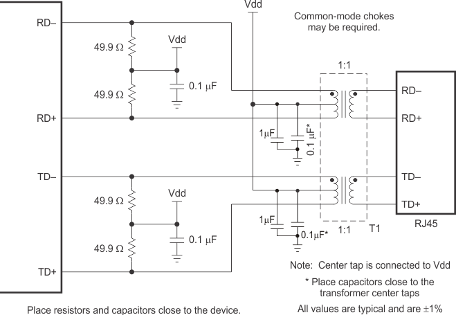 Figure 7-1 10/100Mbs Twisted Pair Interface
7.2 Clock In (XI) Requirements
The TLK111 supports an external CMOS-level oscillator source or an internal oscillator with an external crystal.
7.2.1 Oscillator
If an external clock source is used, XI should be tied to the clock source and XO should be left floating. The amplitude of the oscillator should be a nominal voltage of 3.3V.
7.2.2 Crystal
The use of a 25MHz, parallel, 20pF-load crystal is recommended if a crystal source is desired. Figure 7-2 shows a typical connection for a crystal resonator circuit. The load capacitor values will vary with the crystal vendors; check with the vendor for the recommended loads.
The oscillator circuit is designed to drive a parallel-resonance AT-cut crystal with a minimum drive level of 100μW and a maximum of 500μW. If a crystal is specified for a lower drive level, a current limiting resistor must be placed in series between XO and the crystal.
As a starting point for evaluating an oscillator circuit, if the requirements for the crystal are not known, set the values for CL1 and CL2 at 33pF, and R1 should be set at 0Ω. Specifications for a 25MHz crystal are listed in Table 7-3.
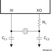 Figure 7-2 Crystal Oscillator Circuit
Table 7-1 25MHz Oscillator Specification
| PARAMETER | TEST CONDITIONS | MIN | TYP | MAX | UNIT |
|---|---|---|---|---|---|
| Frequency | 25 | MHz | |||
| Frequency Tolerance | Operational Temperature | ±50 | ppm | ||
| Frequency Stability | 1 year aging | ±50 | ppm | ||
| Rise / Fall Time | 10%–90% | 8 | nsec | ||
| Jitter (Short term) | Cycle-to-cycle | 50 | psec | ||
| Jitter (Long term) | Accumulative over 10 ms | 1 | nsec | ||
| Symmetry | Duty Cycle | 40% | 60% | ||
| Load Capacitance | 15 | 30 | pF |
Table 7-2 50MHz Oscillator Specification
| PARAMETER | TEST CONDITIONS | MIN | TYP | MAX | UNIT |
|---|---|---|---|---|---|
| Frequency | 50 | MHz | |||
| Frequency Tolerance | Operational Temperature | ±50 | ppm | ||
| Frequency Stability | 1 year aging | ±50 | ppm | ||
| Rise / Fall Time | 10%–90% | 6 | nsec | ||
| Jitter (Short term) | Cycle-to-cycle | 50 | psec | ||
| Jitter (Long term) | Accumulative over 10 ms | 1 | nsec | ||
| Symmetry | Duty Cycle | 40% | 60% |
Table 7-3 25MHz Crystal Specification
| PARAMETER | TEST CONDITIONS | MIN | TYP | MAX | UNIT |
|---|---|---|---|---|---|
| Frequency | 25 | MHz | |||
| Frequency Tolerance | Operational Temperature | ±50 | ppm | ||
| At 25°C | ±50 | ppm | |||
| Frequency Stability | 1 year aging | ±5 | ppm | ||
| Load Capacitance | 10 | 40 | pF |
7.3 Thermal Vias Recommendation
(Extended temperature (125°C) grade only)
The following thermal via guidelines apply to DOWN_PAD, pin 49:
- Thermal via size = 0.2mm
- Recommend 4 vias
- Vias have a center to center separation of 2mm.
Adherence to this guideline is required to achieve the intended operating temperature range of the device. Figure 7-3 illustrates an example layout.
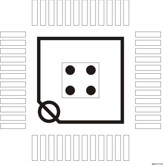 Figure 7-3 Example Layout