SLLSEF8C August 2013 – November 2014 TLK111
PRODUCTION DATA.
- 1 Introduction
- 2 Pin Descriptions
-
3 Hardware Configuration
- 3.1 Bootstrap Configuration
- 3.2 Power Supply Configuration
- 3.3 IO Pins Hi-Z State During Reset
- 3.4 Auto-Negotiation
- 3.5 Auto-MDIX
- 3.6 PHY Address
- 3.7 MII Isolate Mode
- 3.8 Software Strapping Mode
- 3.9 LED Interface
- 3.10 Multi-Configurable LED (MLED)
- 3.11 Loopback Functionality
- 3.12 BIST
- 3.13 Cable Diagnostics
- 4 Interfaces
-
5 Architecture
- 5.1 100Base-TX Transmit Path
- 5.2
100Base-TX Receive Path
- 5.2.1 Analog Front End
- 5.2.2 Adaptive Equalizer
- 5.2.3 Baseline Wander Correction
- 5.2.4 NRZI and MLT-3 Decoding
- 5.2.5 Descrambler
- 5.2.6 5B/4B Decoder and Nibble Alignment
- 5.2.7 Timing Loop and Clock Recovery
- 5.2.8 Phase-Locked Loops (PLL)
- 5.2.9 Link Monitor
- 5.2.10 Signal Detect
- 5.2.11 Bad SSD Detection
- 5.3 10Base-T Receive Path
- 5.4 Auto Negotiation
- 5.5 Link Down Functionality
- 5.6 IEEE 1588 Precision Timing Protocol Support
- 6 Reset and Power Down Operation
- 7 Design Guidelines
-
8 Register Block
- 8.1
Register Definition
- 8.1.1 Basic Mode Control Register (BMCR)
- 8.1.2 Basic Mode Status Register (BMSR)
- 8.1.3 PHY Identifier Register 1 (PHYIDR1)
- 8.1.4 PHY Identifier Register 2 (PHYIDR2)
- 8.1.5 Auto-Negotiation Advertisement Register (ANAR)
- 8.1.6 Auto-Negotiation Link Partner Ability Register (ANLPAR) (BASE Page)
- 8.1.7 Auto-Negotiate Expansion Register (ANER)
- 8.1.8 Auto-Negotiate Next Page Transmit Register (ANNPTR)
- 8.1.9 Auto-Negotiation Link Partner Ability Next Page Register (ANLNPTR)
- 8.1.10 Software Strap Control register 1 (SWSCR1)
- 8.1.11 Software Strap Control register 2 (SWSCR2)
- 8.1.12 Software Strap Control Register 3 (SWSCR3)
- 8.1.13 Extended Register Addressing
- 8.1.14 Fast Link Down Status Register
- 8.1.15 PHY Status Register (PHYSTS)
- 8.1.16 PHY Specific Control Register (PHYSCR)
- 8.1.17 MII Interrupt Status Register 1 (MISR1)
- 8.1.18 MII Interrupt Status Register 2 (MISR2)
- 8.1.19 False Carrier Sense Counter Register (FCSCR)
- 8.1.20 Receiver Error Counter Register (RECR)
- 8.1.21 BIST Control Register (BISCR)
- 8.1.22 RMII Control and Status Register (RCSR)
- 8.1.23 LED Control Register (LEDCR)
- 8.1.24 PHY Control Register (PHYCR)
- 8.1.25 10Base-T Status/Control Register (10BTSCR)
- 8.1.26 BIST Control and Status Register 1 (BICSR1)
- 8.1.27 BIST Control and Status Register2 (BICSR2)
- 8.2 Cable Diagnostic Control Register (CDCR)
- 8.3 PHY Reset Control Register (PHYRCR)
- 8.4 Multi LED Control register (MLEDCR)
- 8.5 IEEE1588 Precision Timing Pin Select (PTPPSEL)
- 8.6 IEEE1588 Precision Timing Configuration (PTPCFG)
- 8.7 TX_CLK Phase Shift Register (TXCPSR)
- 8.8 Power Back Off Control Register (PWRBOCR)
- 8.9 Voltage Regulator Control Register (VRCR)
- 8.10
Cable Diagnostic Configuration/Result Registers
- 8.10.1 ALCD Control and Results 1 (ALCDRR1)
- 8.10.2 Cable Diagnostic Specific Control Registers (CDSCR1 - CDSCR4)
- 8.10.3 Cable Diagnostic Location Results Register 1 (CDLRR1)
- 8.10.4 Cable Diagnostic Location Results Register 2 (CDLRR2)
- 8.10.5 Cable Diagnostic Location Results Register 3 (DDLRR3)
- 8.10.6 Cable Diagnostic Location Results Register 4 (CDLRR4)
- 8.10.7 Cable Diagnostic Location Results Register 5 (CDLRR5)
- 8.10.8 Cable Diagnostic Amplitude Results Register 1 (CDARR1)
- 8.10.9 Cable Diagnostic Amplitude Results Register 2 (CDARR2)
- 8.10.10 Cable Diagnostic Amplitude Results Register 3 (CDARR3)
- 8.10.11 Cable Diagnostic Amplitude Results Register 4 (CDARR4)
- 8.10.12 Cable Diagnostic Amplitude Results Register 5 (CDARR5)
- 8.10.13 Cable Diagnostic General Results Register (CDGRR)
- 8.10.14 ALCD Control and Results 2 (ALCDRR2)
- 8.10.15 ALCD Control and Results 3 (ALCDRR3)
- 8.1
Register Definition
-
9 Electrical Specifications
- 9.1 Absolute Maximum Ratings
- 9.2 Handling Ratings
- 9.3 Recommended Operating ConditionsRedundant row "Power dissipation 200 mW"
- 9.4 48-Pin Industrial Device Thermal Characteristics
- 9.5 48-Pin Extended Temperature (125°C) Device Thermal Characteristics
- 9.6 DC Characteristics, VDD_IO DC Characteristics, SD_IN
- 9.7 DC Characteristics
- 9.8 Power Supply Characteristics
- 9.9
AC Specifications
- 9.9.1 Power Up Timing
- 9.9.2 Reset Timing
- 9.9.3 MII Serial Management Timing
- 9.9.4 100Mb/s MII Transmit Timing
- 9.9.5 100Mb/s MII Receive Timing
- 9.9.6 100Base-TX Transmit Packet Latency Timing
- 9.9.7 100Base-TX Transmit Packet Deassertion Timing
- 9.9.8 100Base-TX Transmit Timing (tR/F and Jitter)
- 9.9.9 100Base-TX Receive Packet Latency Timing
- 9.9.10 100Base-TX Receive Packet Deassertion Timing
- 9.9.11 10Mbs MII Transmit Timing
- 9.9.12 10Mb/s MII Receive Timing
- 9.9.13 10Base-T Transmit Timing (Start of Packet)
- 9.9.14 10Base-T Transmit Timing (End of Packet)
- 9.9.15 10Base-T Receive Timing (Start of Packet)
- 9.9.16 10Base-T Receive Timing (End of Packet)
- 9.9.17 10Mb/s Jabber Timing
- 9.9.18 10Base-T Normal Link Pulse Timing
- 9.9.19 Auto-Negotiation Fast Link Pulse (FLP) Timing
- 9.9.20 100Base-TX Signal Detect Timing
- 9.9.21 100Mbs Loopback Timing
- 9.9.22 10Mbs Internal Loopback Timing
- 9.9.23 RMII Transmit Timing
- 9.9.24 RMII Receive Timing
- 9.9.25 Isolation Timing
- 9.9.26 25MHz_OUT Clock Timing
- 10Revision History, Revision A
3 Hardware Configuration
This section includes information on the various configuration options available with the TLK111. The configuration options described below include:
|
|
3.1 Bootstrap Configuration
Bootstrap configuration is a convenient way to configure the TLK111 into specific modes of operation. Some of the functional pins are used as configuration inputs. The logic states of these pins are sampled during reset and are used to configure the device into specific modes of operation. The table below describes bootstrap configuration.
A 2.2kΩ resistor is used for pull-down or pull-up to change the default configuration. If the default option is desired, then there is no need for external pull-up or pull down resistors. Because these pins may have alternate functions after reset is deasserted, they must not be connected directly to VCC or GND.
| PIN | TYPE | |||||||
|---|---|---|---|---|---|---|---|---|
| NAME | NO. | DESCRIPTION | ||||||
| PHYAD0 (COL) PHYAD1 (RXD_0) PHYAD2 (RXD_1) PHYAD3 (RXD_2) PHYAD4 (RXD_3) |
42 43 44 45 46 |
S, O, PD / PU | PHY Address [4:0]: The TLK111 provides five PHY address pins, the states of which are latched into an internal register at system hardware reset. The TLK111 supports PHY Address values 0 (<00000>) through 31 (<11111>). PHYAD[4:1] pins have weak internal pull-down resistors, and PHYAD[0] has weak internal pull-up resistor, setting the default PHYAD if no external resistors are connected. | |||||
| SW_STRAP | 21 | I | Software Strapping Mode: The TLK111 provides a mechanism to extend the number of configuration pins to allow wider system programmability of PHY functions. An external pull-down will cause the device to enter SW Strapping Mode. In this mode the device will wake up after Power-up or Reset in Power-Down mode, this will allow the system processor to access dedicated Strapping Registers and configure modes of operation. An access to SW Strapping Mode Release register must be done to take the device out of power-down mode. See Section 3.8 for more details. An external pull-up resistor should be used to disable Software Strapping Mode. | |||||
| AN_EN (LED_ACT) AN_1 (LED_SPEED) AN_0 (LED_LINK) |
26 27 28 |
S, O, PU | AN_EN: A high level on this pin puts the part into advertised Auto-Negotiation mode with the capability set by AN_0 and AN_1 pins. A low level on AN_EN puts the part into Forced Mode with the capability set by AN_0 and AN_1 pins. AN_0, AN_1: These input pins control the forced or advertised operating mode according to the following table. The value on these pins is set by connecting the input pins to GND (0) or VCC (1) through 2.2kΩ resistors. DO NOT connect these pins directly to GND or VCC. The states of these pins are latched into the Basic Mode Control Register and the Auto_Negotiation Advertisement Register during Hardware-Reset. The default is 111 because these pins have internal pull-ups. |
|||||
| AN_EN | AN_1 | AN_0 | Forced Mode | |||||
| 0 | 0 | 0 | 10Base-T, Half-Duplex | |||||
| 0 | 0 | 1 | 10Base-T, Full-Duplex | |||||
| 0 | 1 | 0 | 100Base-TX, Half-Duplex | |||||
| 0 | 1 | 1 | 100Base-TX, Full-Duplex | |||||
| AN_EN | AN_1 | AN_0 | Advertised Mode | |||||
| 1 | 0 | 0 | 10Base-T, Half or Full-Duplex | |||||
| 1 | 0 | 1 | 100Base-TX, Half or Full-Duplex | |||||
| 1 | 1 | 0 | 10Base-T, Half-Duplex 100Base-TX, Half-Duplex |
|||||
| 1 | 1 | 1 | 10Base-T, Half orFull-Duplex 100Base-TX, Half or Full-Duplex |
|||||
| LED_CFG (CRS) | 40 | S, O, PU | LED Configuration: This option, along with the LEDCR register bit, selects the mode of operation of the LED pins. Default is Mode 1. All modes are also configurable via register access. See PHY Control Register (PHYCR), Address 0x0019 | |||||
| AMDIX_EN (RX_ER) | 41 | S, O, PU | Auto-MDIX Enable: This option sets the Auto-MDIX mode. By default, it enables Auto-MDIX. An external pull-down resistor disables Auto-MDIX mode. | |||||
| MII_MODE (RX_DV) | 39 | S, O, PD | MII Mode Select: This option selects the operating mode of the MAC data interface. This pin has a weak internal pull-down, and it defaults to normal MII operation mode. An external pull-up causes the device to operate in RMII mode. | |||||
3.2 Power Supply Configuration
The TLK111 provides best-in-class flexibility of power supplies.
3.2.1 Single Supply Operation
If a single 3.3V power supply is desired, the TLK111 internal regulator provides the necessary core supply voltages. Ceramic capacitors of 10µf and 0.1µf should be placed close to the PFBOUT (pin 23) which is the output of the internal regulator. The PFBOUT pin should be connected to the PFBIN1 and PFBIN2 on the board. A small capacitor of 0.1µF should be placed close to the PFBIN1 (pin 18) and PFBIN2 (pin 37). To operate in this mode, connect the TLK111 supply pins as shown in Figure 3-1.
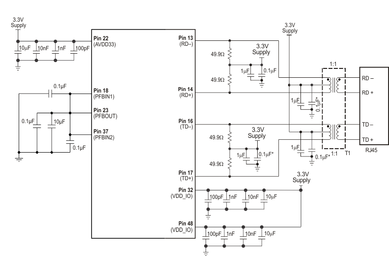 Figure 3-1 Power Connections for Single Supply Operation
3.2.2 Dual Supply Operation
When a 1.55V external power rail is available, the TLK111 can be configured as shown in Figure 3-2. PFBOUT (pin 23) is left floating. The 1.55V external supply is connected to PFBIN1 (pin 18) and PFBIN2 (pin 37). Furthermore, to lower the power consumption, the internal regulator should be powered down by writing ‘1’ to bit 15 of the VRCR register (0x00d0h).
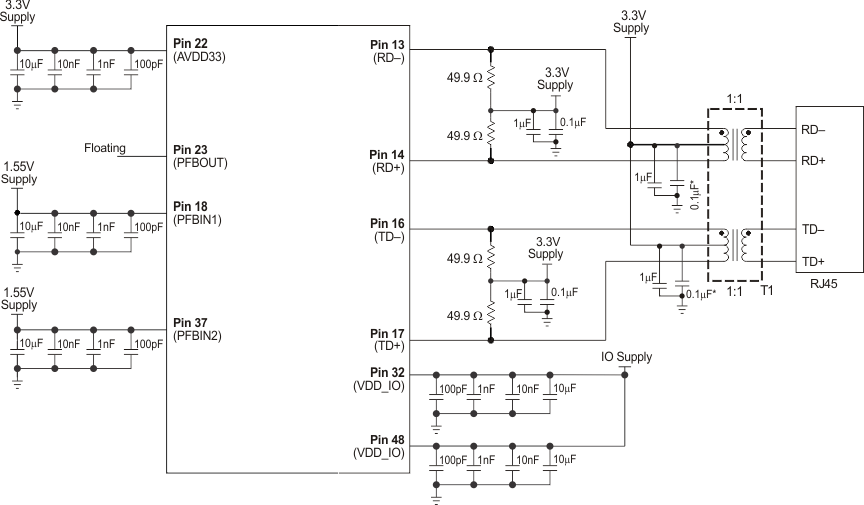 Figure 3-2 Power Connections for Dual Supply Operation
When operating with dual supplies, follow these guidelines:
- When powering up, ramp up the 3.3V supply before the 1.55V supply.
- When powering down, turn off the 1.55V supply before turning off the 3.3V supply.
- Use the external RESET pin after power up to reset the PHY.
- To use the internal power-on reset, PFBIN1 and PFBIN2 must be operational less than 100ms after 3.3V rises to detect the internal RESET.
3.2.3 Variable IO Voltage
The TLK111 digital IO pins can operate with a variable supply voltage. While the primary applications will use 3.3V, VDD_IO can also operate on 2.5V, and for MII mode only, VDD_IO of 1.8V can be used as well. For more details, see Section 9.6.
3.3 IO Pins Hi-Z State During Reset
The following IO or output pins are in hi-Z state when RESET is active (Low).
| Pin Name | Type | Internal PU/PD | Pin Name | Type | Internal PU/PD | |
|---|---|---|---|---|---|---|
| TXD_3 | IO | PD | RX_ER | IO | PU | |
| TX_EN | IO | PD | COL | IO | PU | |
| INT/PWDN | IO | PU | RXD_0 | IO | PD | |
| LED_ACT | IO | PU | RXD_1 | IO | PD | |
| LED_SPEED | IO | PU | RXD_2 | IO | PD | |
| LED_LINK | IO | PU | RXD_3 | IO | PD | |
| MDIO | IO | TX_CLK | O | |||
| RX_DV | IO | PD | CLK25MHz_OUT | O | ||
| CRS | IO | PU | RX_CLK | O |
3.4 Auto-Negotiation
The TLK111 device auto-negotiates to operate in 10Base-T or 100Base-TX. With Auto-Negotiation enabled, the TLK111 negotiates with the link partner to determine the speed and duplex mode. If the link partner cannot Auto-Negotiate, the TLK111 device enters parallel-detect mode to determine the speed of the link partner. Parallel-detect mode uses fixed half-duplex mode.
The TLK111 supports four different Ethernet protocols (10Mbs Half-Duplex, 10Mbs Full-Duplex, 100Mbs Half-Duplex, and 100Mbs Full-Duplex). Auto-Negotiation selects the highest performance protocol based on the advertised ability of the Link Partner. Control the Auto-Negotiation function within the TLK111 by:
- Internal register access, or
- Configuring the AN_EN, AN_1 and AN_0 pins
The state of the AN_EN, AN_0 and AN_1 pins determine whether the TLK111 is forced into a specific mode, or if Auto-Negotiation advertises a specific ability (or set of abilities) as given in Table 3-1. These pins allow configuration options to be selected without requiring internal register access. The state of AN_EN, AN_0 and AN_1, upon power-up/reset, determines the state of bits [8:5] of the ANAR register (0x04h).
Internal register access controls the Auto-Negotiation function, as defined by the IEEE 802.3u specification. For further detail regarding Auto-Negotiation, see Clause 28 of the IEEE 802.3u specification.
Table 3-1 Auto-Negotiation Modes
| AN_EN | AN_1 | AN_0 | Forced Mode |
|---|---|---|---|
| 0 | 0 | 0 | 10Base-T, Half-Duplex |
| 0 | 0 | 1 | 10Base-T, Full-Duplex |
| 0 | 1 | 0 | 100Base-TX, Half-Duplex |
| 0 | 1 | 1 | 100Base-TX, Full-Duplex |
| AN_EN | AN_1 | AN_0 | Advertised Mode |
| 1 | 0 | 0 | 10Base-T, Half or Full-Duplex |
| 1 | 0 | 1 | 100Base-TX, Half or Full-Duplex |
| 1 | 1 | 0 | 10Base-T, Half Duplex 100Base-TX, Half Duplex |
| 1 | 1 | 1 | 10Base-T, Half or Full-Duplex 100Base-TX, Half or Full-Duplex |
3.5 Auto-MDIX
The TLK111 device automatically determines whether or not it needs to cross over between pairs, eliminating the requirement for an external crossover cable. If the TLK111 interoperates with a device that implements MDI/MDIX crossover, a random algorithm as described in IEEE 802.3 determines which device performs the crossover.
Auto-MDIX is enabled by default and can be configured via pin strap, SW Strap register SWSCR1 (0x09h), bit 14 or via register PHYCR (0x19h), bit 15.
The crossover can be manually forced through bit 14 of the PHYCR (0x19h) register. Neither Auto-Negotiation nor Auto-MDIX is required to be enabled in forcing crossover of the MDI pairs.
Auto-MDIX can be used in the forced 100Base-TX mode. Because in modern networks all the nodes are 100Base-TX, having the Auto-MDIX working in the forced 100Base-TX mode resolves the link faster without the need for the long Auto-Negotiation period.
3.6 PHY Address
The 5 PHY address inputs pins are shared with the RXD[3:0] pins and COL pin as shown in Table 3-2.
Table 3-2 PHY Address Mapping
| PIN Number | PHYAD FUNCTION | RXD FUNCTION |
|---|---|---|
| 42 | PHYAD0 | COL |
| 43 | PHYAD1 | RXD_0 |
| 44 | PHYAD2 | RXD_1 |
| 45 | PHYAD3 | RXD_2 |
| 46 | PHYAD4 | RXD_3 |
Each TLK111 or port sharing an MDIO bus in a system must have a unique physical address. With 5 address input pins, the TLK111 can support PHY Address values 0 (<00000>) through 31 (<11111>). The address-pin states are latched into an internal register at device power-up and hardware reset. Because all the PHYAD[4:0] pins have weak internal pull-down/up resistors, the default setting for the PHY address is 00001 (0x01h).
See Figure 3-3 for an example of a PHYAD connection to external components. In this example, the PHYAD configuration results in address 00011 (0x03h).
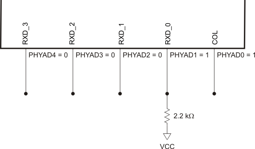 Figure 3-3 PHYAD Configuration Example
3.7 MII Isolate Mode
The TLK111 can be put into MII-Isolate mode by writing bit 10 of the BMCR register.
When in the MII-Isolate mode, the TLK111 ignores packet data present at the TXD[3:0], TX_EN inputs, and presents a high impedance on the TX_CLK, RX_CLK, RX_DV, RX_ER, RXD[3:0], COL, and CRS outputs. When in isolate mode, the TLK111 continues to respond to all management transactions.
When in isolate mode, the PMD output pair does not transmit packet data, but continues to source 100Base-TX scrambled idles or 10Base-T normal link pulses. The TLK111 can auto-negotiate or parallel detect on the receive signal at the PMD input pair. A valid link can be established for the receiver even when the TLK111 is in Isolate mode.
3.8 Software Strapping Mode
The TLK111 provides a mechanism to extend the number of configuration pins to allow wider system programmability of PHY functions.
Connecting an external pull-down to pin 21 causes the device to enter SW Strapping Mode after power-up or a hardware reset event. In this mode the device wakes up after power-up/hardware reset in power down mode. While in power down (in SW strap mode only) the PHY allows the system processor to access the dedicated Strapping Registers and configure modes of operation. Once the dedicated Strapping Registers are programmed, setting the SW Strapping Mode Release register bit (“Configuration done”), bit 15 of register SWSCR1(0x0009), must be done in order to take the device out of power-down mode. An internal reset pulse is generated and the SW Strap Register values are latched into internal registers. Unless a new Power-up/HW reset was applied, the configured SW Strap Register values will function as default values. Generation of Software Reset/Software Restart - bits 15 and 14 of register PHYRCR (0x001F) will not clear the configured SW Strap bit values.
There are 3 Software Strapping control registers: SWSCR1 (0x0009), SWSCR2 (0x000A) and SWSCR3(0x000B) contain the configuration bits used as strapping options or virtual strapping pins during HW Reset or Power-Up.
The TLK111 Software Strap mechanism behavior is shown in Figure 3-4.
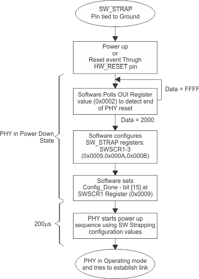
Figure 3-5 shows the timing relationship for typical SW Strapping programming.
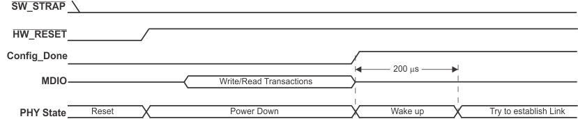 Figure 3-5 TLK111 SW Strap Timing Diagram
Connecting an external pull-up resistor to pin 21 disables Software Strapping Mode during power up or HW Reset.
3.9 LED Interface
The TLK111 supports three configurable Light Emitting Diode (LED) pins. The device supports three LED configurations: Link, Speed, and Activity. Functions are multiplexed among the LEDs into three modes. The LEDs can be controlled by configuration pin and-or internal register bits. Bits 6:5 of the PHY Control register (PHYCR) selects the LED mode as described in Table 3-3.
Table 3-3 LED Mode Select
| Mode | LED_CFG[1] (bit 6) |
LED_CFG[0] (bit 5) or (pin 40) |
LED_LINK | LED_SPEED | LED_ACT |
|---|---|---|---|---|---|
| 1 | don't care | 1 | ON for Good Link OFF for No Link |
ON in 100Mbs OFF in 10Mbs |
ON Pulse for Activity OFF for No Activity |
| 2 | 0 | 0 | ON for Good Link BLINK for Activity |
ON in 100Mbs OFF in 10Mbs |
ON for Collision OFF for No Collision |
| 3 | 1 | 0 | ON for Good Link BLINK for Activity |
ON in 100Mbs OFF in 10Mbs |
ON for Full Duplex OFF for Half Duplex |
The LED_LINK pin in Mode 1 indicates the link status of the port. The LED is OFF when no link is present. In Mode 2 and Mode 3 it is ON to indicate that the link is good; BLINK indicates that activity is present on either transmit or receive channel. Bits 10:9 of the LEDCR register (0x18) control the blink rate. The default blink rate is 5Hz.
The LED_SPEED pin indicates the data rate of the port, 10Mbs or 100Mbs. This LED is ON when the device is operating in 100Mbs operation. The functionality of this LED is independent of mode selected.
The LED_ACT pin in Mode 1 indicates the presence of either transmit or receive activity. The LED is ON (Pulse) for Activity and OFF for No Activity. In mode 2 this pin indicates the collision status of the port. The LED is ON when there is a collision and OFF when there is no collision. In mode 3 this pin indicates the Duplex status of operation. The LED is ON for Full Duplex and OFF for Half Duplex.
Bits 8:6 of the LEDCR register define the polarity of the signals on the LED pins.
Because the Auto-Negotiation (AN) configuration options share the LED output pins, the external components required for configuration-pin programming and those for LED usage must be considered in order to avoid contention.
See Figure 3-6 for an example of AN_0, AN_1, AN_EN connections to external components. In this example, the configuration results in Auto-Negotiation with 10/100 Full-Duplex advertised.
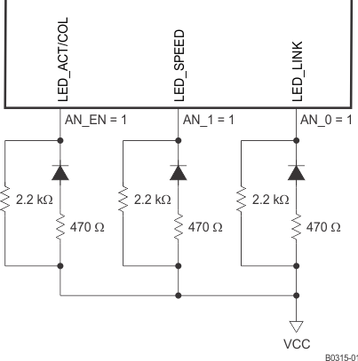 Figure 3-6 AN Pin Configuration and LED Loading Example
3.10 Multi-Configurable LED (MLED)
In addition, the TLK111 supports by register access a multi-configurable LED (MLED). The MLED by default is not activated; by register access it can be routed through either the 3 LED pins 26-28 or the COL pin, allowing support of 4 LEDS. When MLED is routed to the COL pin, the COL functionality is disabled. REG 0x0025 (MLEDCR Register) controls the MLED routing and configurations. The different MLED modes are configured by bits [6:3] as described in Table 3-4.
Table 3-4 MLED Mode Select
|
(bit 6:3) |
Mode | (bit 6:3) | Mode | |
|---|---|---|---|---|
| 0x0 | Link OK | 0x6 | LED Speed: High for 10 Base TX | |
| 0x1 | RX/TX Activity | 0x7 | Full Duplex | |
| 0x2 | TX Activity | 0x8 | Link OK / Blink on TX/RX Activity | |
| 0x3 | RX Activity | 0x9 | Active stretch signal | |
| 0x4 | Collision | 0xA | MI_LINK (100BT+FD) | |
| 0x5 | LED Speed: High for 100 Base TX |
3.11 Loopback Functionality
The TLK111 provides several options for Loopback that test and verify various functional blocks within the PHY. Enabling loopback mode allows in-circuit testing of the TLK111 digital and analog data path. Generally, the TLK111 may be configured to one of the Near-end loopback modes or to the Far-end (reverse) loopback.
3.11.1 Near-End Loopback
Near-end loopback provides the ability to loop the transmitted data back to the receiver via the digital or analog circuitry. The point at which the signal is looped back is selected using loopback control bits with several options being provided. Figure 3-7 shows the PHY near-end loopback functionality.
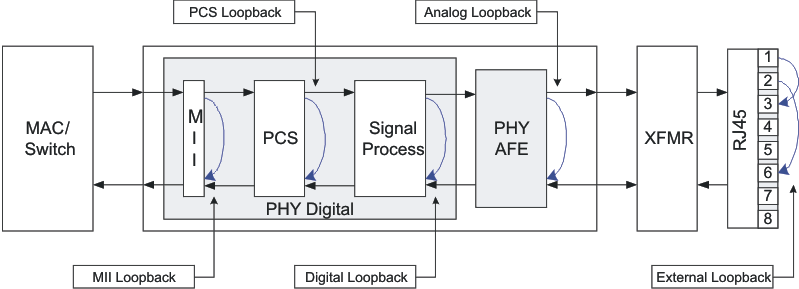 Figure 3-7 Block Diagram, Near-End Loopback Mode
The Near-end Loopback mode is selected by setting the respective bit in the BIST Control Register (BISCR), MII register address 0x0016. MII loopback can be selected by using the BMCR register at address 0x0000, bit [14].
- Reg 0x0000, Bit [14]: MII Loopback
- Reg 0x0016, Bit [0]: PCS input Loopback
- Reg 0x0016, Bit [1]: PCS output Loopback
- Reg 0x0016, Bit [2]: Digital Loopback
- Reg 0x0016, Bit [3]: Analog Loopback
The Near-end Loopback can be selected according to the following:
Table 3-5 describes the available operational modes for each loop mode:
Table 3-5 Loop Modes
| Loop Mode | MII | PCS Input | PCS Output | Digital | Analog(1) | External |
|---|---|---|---|---|---|---|
| Operational Setting | Force/ANEG 100/10 | Force 100/10 | Force 100 | Force 100 | Force 10/100 ANEG 10 | Force/ANEG 100/10 |
| Operational MAC int. | MII Only | MII or RMII | MII or RMII | MII or RMII | MII or RMII | MII or RMII |
While in MII Loopback mode, there is no link indication, but packets propagate back to the MAC. While in MII Loopback mode the data is looped back, and can also be transmitted onto the media. For transmitting data during MII loopback in 100BT only please use bit [6] in the BISCR Register address 0x0016. For proper operation in Analog Loopback mode, attach 100Ω terminations to the RJ45 connector. External Loopback can be performed while working in normal mode (Bits 3:0 of the BISCR register are asserted to 0, and on the RJ45 connector, pin 1 is connected to pin 3 and pin 2 is connected to pin 6). To maintain the desired operating mode, Auto-Negotiation should be disabled before selecting Loopback mode. This constraint does not apply for external-loopback mode. For selected loopback Delay propagation timing please see Section 9.9.21.
3.11.2 Far-End Loopback
Far-end (Reverse) loopback is a special test mode to allow testing the PHY from the link-partner side. In this mode, data that is received from the link partner passes through the PHY's receiver, looped back on the MII and transmitted back to the link partner. Figure 3-8 shows Far-end loopback functionality.
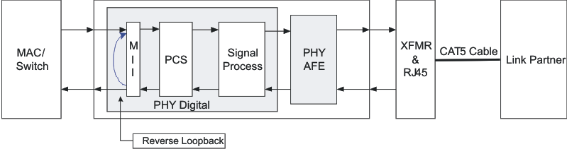 Figure 3-8 Block Diagram, Far-End Loopback Mode
The Reverse Loopback mode is selected by setting bit 4 in the BIST Control Register (BISCR), MII register address 0x0016.
While in Reverse Loopback mode the data is looped back and also transmitted onto the MAC Interface and all data signals that come from the MAC are ignored.
Table 3-6 describes the operating modes for Far-End Loopback.
Table 3-6 Far-End Loopback Modes
| Operational MAC Int. | MII Mode | RMII Mode |
|---|---|---|
| Operational Setting | Force/ANEG 10/100 | Force/ANEG 10 |
3.12 BIST
The device incorporates an internal PRBS Built-in Self Test (BIST) circuit to accommodate in-circuit testing or diagnostics. The BIST circuit can be used to test the integrity of the transmit and receive data paths. The BIST can be performed using both internal loopback (digital or analog) or external loopback using a cable fixture. The BIST simulates pseudo-random data transfer scenarios in format of real packets and Inter-Packet Gap (IPG) on the lines. The BIST allows full control of the packet lengths and of the IPG.
The BIST is implemented with independent transmit and receive paths, with the transmit block generating a continuous stream of a pseudo-random sequence. The device generates a 15-bit pseudo-random sequence for the BIST. The received data is compared to the generated pseudo-random data by the BIST Linear Feedback Shift Register (LFSR) to determine the BIST pass/fail status. The number of error bytes that the PRBS checker received is stored in the BICSR1 register (0x001Bh). The status of whether the PRBS checker is locked to the incoming receive bit stream, whether the PRBS has lost sync, and whether the packet generator is busy, can be read from the BISCR register (0x0016h). While the lock and sync indications are required to identify the beginning of proper data reception, for any link failures or data corruption, the best indication is the contents of the the error counter in the BICSR1 register (0x001Bh).
The PRBS test can be put in a continuous mode or single mode by using bit 14 of the BISCR register (0x0016h). In continuous mode, when one of the PRBS counters reaches the maximum value, the counter starts counting from zero again. In single mode, when the PRBS counter reaches its maximum value, the PRBS checker stops counting.
The device allows the user to control the length of the PRBS packet. By programming the BICSR2 register (0x001Ch) one can set the length of the PRBS packet. There is also an option to generate a single-packet transmission of two types, 64 and 1518 bytes, through register bit 13 of the BISCR register (0x0016h). The single generated packet is composed of a constant data.
3.13 Cable Diagnostics
With the vast deployment of Ethernet devices, the need for reliable, comprehensive and user-friendly cable diagnostic tool is more important than ever. The wide variety of cables, topologies, and connectors deployed results in the need to non-intrusively identify and report cable faults. The TI cable-diagnostic unit provides extensive information about cable integrity.
The TLK111 offers the following capabilities in its Cable Diagnostic tools kit:
- Time Domain Reflectometry (TDR)
- Active Link Cable Diagnostic (ALCD)
3.13.1 TDR
The TLK111 uses Time Domain Reflectometry (TDR) to determine the quality of the cables, connectors, and terminations in addition to estimating the cable length. Some of the possible problems that can be diagnosed include opens, shorts, cable impedance mismatch, bad connectors, termination mismatches, cross faults, cross shorts and any other discontinuities along the cable.
The TLK111 transmits a test pulse of known amplitude (1V or 2.5V) down each of the two pairs of an attached cable. The transmitted signal continues down the cable and reflects from each cable imperfection, fault, bad connector, and from the end of the cable itself. After the pulse transmission the TLK111 measures the return time and amplitude of all these reflected pulses. This technique enables measuring the distance and magnitude (impedance) of non-terminated cables (open or short), discontinuities (bad connectors), and improperly-terminated cables with ±1m accuracy.
The TLK111 also uses data averaging to reduce noise and improve accuracy. The TLK111 can record up to five reflections within the tested pair. If more than 5 reflections are recorded, the TLK111 saves the first 5 of them. If a cross fault is detected, the TDR saves the first location of the cross fault and up to 4 reflections in the tested channel. The TLK111 TDR can measure cables up to 200m in length.
For all TDR measurements, the transformation between time of arrival and physical distance is done by the external host using minor computations (such as multiplication, addition and lookup tables). The host must know the expected propagation delay of the cable, which depends, among other things, on the cable category (for example, CAT5, CAT5e, or CAT6).
TDR measurement is allowed in the TLK111 in the following scenarios:
- While Link partner is disconnected – cable is unplugged at the other side
- Link partner is connected but remains “quiet” (for example, in power down mode)
- TDR could be automatically activated when the link fails or is dropped by setting bit 8 of register 0x0009 (SWSCR1). The results of the TDR run after the link fails will be saved in the TDR registers. The SW could read these registers at any time to apply post processing on the TDR results. This mode is designed for cases in which the link dropped due to cable disconnections, in which after link failure, the line will be quiet to allow a proper function of the TDR.
3.13.2 ALCD
The TLK111 also supports Active Link Cable Diagnostic (ALCD). The ALCD offers a passive method to estimate the cable length during active link. The ALCD uses passive digital signal processing based on adapted data, thus enabling measurement of cable length with an active link partner.
The ALCD Cable length measurement accuracy is ±5m for the pair used in the Rx path (due to the passive nature of the test, only the receive path is measured).