SLLSEF8C August 2013 – November 2014 TLK111
PRODUCTION DATA.
- 1 Introduction
- 2 Pin Descriptions
-
3 Hardware Configuration
- 3.1 Bootstrap Configuration
- 3.2 Power Supply Configuration
- 3.3 IO Pins Hi-Z State During Reset
- 3.4 Auto-Negotiation
- 3.5 Auto-MDIX
- 3.6 PHY Address
- 3.7 MII Isolate Mode
- 3.8 Software Strapping Mode
- 3.9 LED Interface
- 3.10 Multi-Configurable LED (MLED)
- 3.11 Loopback Functionality
- 3.12 BIST
- 3.13 Cable Diagnostics
- 4 Interfaces
-
5 Architecture
- 5.1 100Base-TX Transmit Path
- 5.2
100Base-TX Receive Path
- 5.2.1 Analog Front End
- 5.2.2 Adaptive Equalizer
- 5.2.3 Baseline Wander Correction
- 5.2.4 NRZI and MLT-3 Decoding
- 5.2.5 Descrambler
- 5.2.6 5B/4B Decoder and Nibble Alignment
- 5.2.7 Timing Loop and Clock Recovery
- 5.2.8 Phase-Locked Loops (PLL)
- 5.2.9 Link Monitor
- 5.2.10 Signal Detect
- 5.2.11 Bad SSD Detection
- 5.3 10Base-T Receive Path
- 5.4 Auto Negotiation
- 5.5 Link Down Functionality
- 5.6 IEEE 1588 Precision Timing Protocol Support
- 6 Reset and Power Down Operation
- 7 Design Guidelines
-
8 Register Block
- 8.1
Register Definition
- 8.1.1 Basic Mode Control Register (BMCR)
- 8.1.2 Basic Mode Status Register (BMSR)
- 8.1.3 PHY Identifier Register 1 (PHYIDR1)
- 8.1.4 PHY Identifier Register 2 (PHYIDR2)
- 8.1.5 Auto-Negotiation Advertisement Register (ANAR)
- 8.1.6 Auto-Negotiation Link Partner Ability Register (ANLPAR) (BASE Page)
- 8.1.7 Auto-Negotiate Expansion Register (ANER)
- 8.1.8 Auto-Negotiate Next Page Transmit Register (ANNPTR)
- 8.1.9 Auto-Negotiation Link Partner Ability Next Page Register (ANLNPTR)
- 8.1.10 Software Strap Control register 1 (SWSCR1)
- 8.1.11 Software Strap Control register 2 (SWSCR2)
- 8.1.12 Software Strap Control Register 3 (SWSCR3)
- 8.1.13 Extended Register Addressing
- 8.1.14 Fast Link Down Status Register
- 8.1.15 PHY Status Register (PHYSTS)
- 8.1.16 PHY Specific Control Register (PHYSCR)
- 8.1.17 MII Interrupt Status Register 1 (MISR1)
- 8.1.18 MII Interrupt Status Register 2 (MISR2)
- 8.1.19 False Carrier Sense Counter Register (FCSCR)
- 8.1.20 Receiver Error Counter Register (RECR)
- 8.1.21 BIST Control Register (BISCR)
- 8.1.22 RMII Control and Status Register (RCSR)
- 8.1.23 LED Control Register (LEDCR)
- 8.1.24 PHY Control Register (PHYCR)
- 8.1.25 10Base-T Status/Control Register (10BTSCR)
- 8.1.26 BIST Control and Status Register 1 (BICSR1)
- 8.1.27 BIST Control and Status Register2 (BICSR2)
- 8.2 Cable Diagnostic Control Register (CDCR)
- 8.3 PHY Reset Control Register (PHYRCR)
- 8.4 Multi LED Control register (MLEDCR)
- 8.5 IEEE1588 Precision Timing Pin Select (PTPPSEL)
- 8.6 IEEE1588 Precision Timing Configuration (PTPCFG)
- 8.7 TX_CLK Phase Shift Register (TXCPSR)
- 8.8 Power Back Off Control Register (PWRBOCR)
- 8.9 Voltage Regulator Control Register (VRCR)
- 8.10
Cable Diagnostic Configuration/Result Registers
- 8.10.1 ALCD Control and Results 1 (ALCDRR1)
- 8.10.2 Cable Diagnostic Specific Control Registers (CDSCR1 - CDSCR4)
- 8.10.3 Cable Diagnostic Location Results Register 1 (CDLRR1)
- 8.10.4 Cable Diagnostic Location Results Register 2 (CDLRR2)
- 8.10.5 Cable Diagnostic Location Results Register 3 (DDLRR3)
- 8.10.6 Cable Diagnostic Location Results Register 4 (CDLRR4)
- 8.10.7 Cable Diagnostic Location Results Register 5 (CDLRR5)
- 8.10.8 Cable Diagnostic Amplitude Results Register 1 (CDARR1)
- 8.10.9 Cable Diagnostic Amplitude Results Register 2 (CDARR2)
- 8.10.10 Cable Diagnostic Amplitude Results Register 3 (CDARR3)
- 8.10.11 Cable Diagnostic Amplitude Results Register 4 (CDARR4)
- 8.10.12 Cable Diagnostic Amplitude Results Register 5 (CDARR5)
- 8.10.13 Cable Diagnostic General Results Register (CDGRR)
- 8.10.14 ALCD Control and Results 2 (ALCDRR2)
- 8.10.15 ALCD Control and Results 3 (ALCDRR3)
- 8.1
Register Definition
-
9 Electrical Specifications
- 9.1 Absolute Maximum Ratings
- 9.2 Handling Ratings
- 9.3 Recommended Operating ConditionsRedundant row "Power dissipation 200 mW"
- 9.4 48-Pin Industrial Device Thermal Characteristics
- 9.5 48-Pin Extended Temperature (125°C) Device Thermal Characteristics
- 9.6 DC Characteristics, VDD_IO DC Characteristics, SD_IN
- 9.7 DC Characteristics
- 9.8 Power Supply Characteristics
- 9.9
AC Specifications
- 9.9.1 Power Up Timing
- 9.9.2 Reset Timing
- 9.9.3 MII Serial Management Timing
- 9.9.4 100Mb/s MII Transmit Timing
- 9.9.5 100Mb/s MII Receive Timing
- 9.9.6 100Base-TX Transmit Packet Latency Timing
- 9.9.7 100Base-TX Transmit Packet Deassertion Timing
- 9.9.8 100Base-TX Transmit Timing (tR/F and Jitter)
- 9.9.9 100Base-TX Receive Packet Latency Timing
- 9.9.10 100Base-TX Receive Packet Deassertion Timing
- 9.9.11 10Mbs MII Transmit Timing
- 9.9.12 10Mb/s MII Receive Timing
- 9.9.13 10Base-T Transmit Timing (Start of Packet)
- 9.9.14 10Base-T Transmit Timing (End of Packet)
- 9.9.15 10Base-T Receive Timing (Start of Packet)
- 9.9.16 10Base-T Receive Timing (End of Packet)
- 9.9.17 10Mb/s Jabber Timing
- 9.9.18 10Base-T Normal Link Pulse Timing
- 9.9.19 Auto-Negotiation Fast Link Pulse (FLP) Timing
- 9.9.20 100Base-TX Signal Detect Timing
- 9.9.21 100Mbs Loopback Timing
- 9.9.22 10Mbs Internal Loopback Timing
- 9.9.23 RMII Transmit Timing
- 9.9.24 RMII Receive Timing
- 9.9.25 Isolation Timing
- 9.9.26 25MHz_OUT Clock Timing
- 10Revision History, Revision A
4 Interfaces
4.1 Media Independent Interface (MII)
The Media Independent Interface (MII) is a synchronous 4-bit wide nibble data interface that connects the PHY to the MAC in 100B-TX and 10B-T modes. The MII is fully compliant with IEEE802.3-2002 clause 22.
The MII signals are summarized below.
| Data signals | TXD [3:0] | ||
| RXD [3:0] | |||
| Transmit and receive-valid signals | TX_EN | ||
| RX_DV | |||
| Line-status signals | CRS (carrier sense) | ||
| COL (collision) |
Figure 4-1 shows the MII-mode signals.
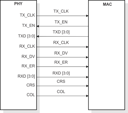 Figure 4-1 MII Signaling
The Isolate bit (BMCR register bit 10), defined in IEEE802.3-2002, electrically isolates the PHY from the MII (if set, all transactions on the MII interface are ignored by the PHY).
Additionally, the MII interface includes the carrier sense signal CRS, as well as a collision detect signal COL. The CRS signal asserts to indicate the reception of data from the network or as a function of transmit data in Half Duplex mode. The COL signal asserts as an indication of a collision which can occur during half-duplex operation when both transmit and receive operation occur simultaneously.
4.2 Reduced Media Independent Interface (RMII)
TLK111 incorporates the Reduced Media Independent Interface (RMII) as specified in the RMII specification (rev1.2) from the RMII consortium. The purpose of this interface is to provide a low cost alternative to the IEEE 802.3u MII as specified in Clause 22. Architecturally, the RMII specification provides an additional reconciliation layer on either side of the MII, but can be implemented in the absence of an MII.
The RMII specification has the following characteristics:
- Supports 10Mbs and 100Mbs data rates
- Single clock reference sourced from the MAC to PHY (or from an external source)
- Provides independent 2 bit wide (di-bit) transmit and receive data paths
- Uses CMOS signal levels, the same levels as the MII interface
In this mode, data transfers two bits at a time using the 50MHz RMII reference clock for both transmit and receive. RMII mode uses the following pins:
| Signal | Pin |
| XI (RMII reference clock is 50MHz) | 34 |
| TXD_0 | 3 |
| TXD_1 | 4 |
| TX_EN | 2 |
| CRS_DV | 40 |
| RX_ER | 41 |
| RXD_0 | 43 |
| RXD_1 | 44 |
Data on TXD [1:0] are latched at the PHY with reference to the reference-clock edges on the XI pin. Data on RXD [1:0] are latched at the MAC with reference to the same reference clock edges on the XI pin. The RMII operates at the same speed (50MHz) in both 10B-T and 100B-TX. In 10B-T the data is 10 times slower than the reference clock, so transmit data is sampled every 10 clocks. Likewise, receive data is generated on every 10th clock so that an attached MAC device can sample the data every 10 clocks.
In addition, RMII mode supplies an RX_DV signal which allows a simpler method of recovering receive data without the need to separate RX_DV from the CRS_DV indication. RX_ER is also supported even though not required by RMII spec (The TLK111 supports optional use of RX_ER and RX_DV in RMII as an extra feature). RMII mode requires a 50MHz oscillator connected to the device XI pin.
The TLK111 supports a special mode called “RMII receive clock” mode. This mode, which is not part of the RMII specification, allows synchronization of the MAC-PHY RX interface. In this mode, the PHY generates a recovered 50MHz clock through the RX_CLK pin and synchronizes the RXD[1:0], CRS_DV, RX_DV and RX_ER signals to this clock. Setting register 0x000A bit [0] is required to activate this mode.
Figure 4-2 describes the RMII signals connectivity between the TLK111 and any MAC device.
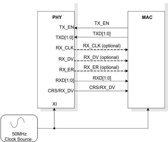 Figure 4-2 TLK111 RMII/MAC Connection
RMII function includes a programmable elastic buffer to adjust for the frequency differences between the reference clock and the recovered receive clock. The programmable elastic buffer minimizes internal propagation delay based on expected maximum packet size and clock accuracy.
Table 4-1 indicates how to program the buffer FIFO based on the expected max packet size and clock accuracy. It assumes that the RMII reference clock and the far-end transmitter clock have the same accuracy.
Table 4-1 Recommended RMII Packet Sizes
| Start Threshold RBR[1:0] | Latency Tolerance | Recommended packet size at ±50ppm | Recommended packet size at ±100ppm |
|---|---|---|---|
| 1(4-bits) | 2 bits | 2400 bytes | 1200 bytes |
| 2(8-bits) | 6 bits | 7200 bytes | 3600 bytes |
| 3(12-bits) | 10 bits | 12000 bytes | 6000 bytes |
| 0(16-bits) | 14 bits | 16800 bytes | 8400 bytes |
4.3 Serial Management Interface
The Serial Management Interface (SMI), provides access to the TLK111 internal register space for status information and configuration. The SMI is compatible with IEEE802.3-2002 clause 22. The implemented register set consists of all the registers required by the IEEE802.3-2002, plus several others to provide additional visibility and controllability of the TLK111 device.
The SMI includes the MDC management clock input and the management MDIO data pin. The MDC clock is sourced by the external management entity, also called Station (STA), and can run at a maximum clock rate of 25MHz. MDC is not expected to be continuous, and can be turned off by the external management entity when the bus is idle.
The MDIO is sourced by the external management entity and by the PHY. The data on the MDIO pin is latched on the rising edge of the MDC clock. The MDIO pin requires a pull-up resistor (2.2kΩ) which, during IDLE and turnaround, pulls MDIO high.
Up to 32 PHYs can share a common SMI bus. To distinguish between the PHYs, a 5-bit address is used. During power-up reset, the TLK111 latches the PHYAD[4:0] configuration pins (Pin 42 to Pin 46) to determine its address.
The management entity must not start an SMI transaction in the first cycle after power-up reset. To maintain valid operation, the SMI bus must remain inactive at least one MDC cycle after hard reset is de-asserted.
In normal MDIO transactions, the register address is taken directly from the management-frame reg_addr field, thus allowing direct access to 32 16-bit registers (including those defined in IEEE802.3 and vendor specific). The data field is used for both reading and writing. The Start code is indicated by a <01> pattern. This pattern makes sure that the MDIO line transitions from the default idle line state. Turnaround is defined as an idle bit time inserted between the Register Address field and the Data field. To avoid contention during a read transaction, no device may actively drive the MDIO signal during the first bit of Turnaround. The addressed TLK111 drives the MDIO with a zero for the second bit of turnaround and follows this with the required data. Figure 4-3 shows the timing relationship between MDC and the MDIO as driven/received by the Station (STA) and the TLK111 (PHY) for a typical register read access.
For write transactions, the station-management entity writes data to the addressed TLK111, thus eliminating the requirement for MDIO Turnaround. The Turnaround time is filled by the management entity by inserting <10>. Figure 4-4 shows the timing relationship for a typical MII register write access. The frame structure and general read/write transactions are shown in Table 4-2, Figure 4-3, and Figure 4-4.
Table 4-2 Typical MDIO Frame Format
| MII Management Serial Protocol | <idle><start><op code><device addr><reg addr><turnaround><data><idle> |
|---|---|
| Read Operation | <idle><01><10><AAAAA><RRRRR><Z0><xxxx xxxx xxxx xxxx><idle> |
| Write Operation | <idle><01><01><AAAAA><RRRRR><10><xxxx xxxx xxxx xxxx><idle> |
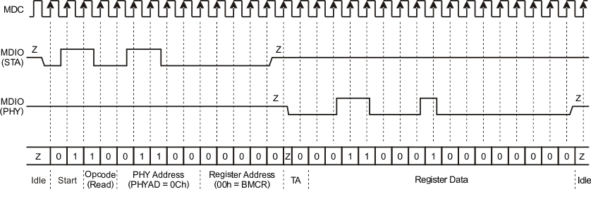 Figure 4-3 Typical MDC/MDIO Read Operation
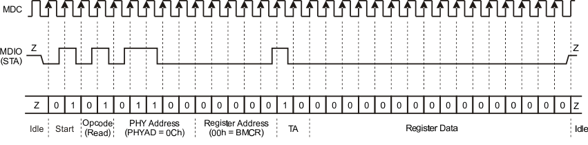 Figure 4-4 Typical MDC/MDIO Write Operation
4.3.1 Extended Address Space Access
The TLK111 SMI function supports read/write access to the extended register set using registers REGCR(0x000Dh) and ADDAR(0x000Eh) and the MDIO Manageable Device (MMD) indirect method defined in IEEE802.3ah Draft for clause 22 for accessing the clause 45 extended register set.
The standard register set, MDIO registers 0 to 31, is accessed using the normal direct-MDIO access or the indirect method, except for register REGCR(0x000Dh) and ADDAR(0x000Eh) which is accessed only using the normal MDIO transaction. The SMI function will ignore indirect accesses to these registers.
REGCR(0x000Dh) is the MDIO Manageable MMD access control. In general, register REGCR(4:0) is the device address DEVAD that directs any accesses of ADDAR(0x000Eh) register to the appropriate MMD. Specifically, the TLK111 uses the vendor-specific DEVAD[4:0] = "11111" for accesses. All accesses through registers REGCR and ADDAR must use this DEVAD. Transactions with other DEVAD are ignored. REGCR[15:14] holds the access function: address (00), data with no post increment (01), data with post increment on read and writes (10) and data with post increment on writes only (11).
- ADDAR is the address/data MMD register. ADDAR is used in conjunction with REGCR to provide the access to the extended register set. If register REGCR[15:1] is 00, then ADDAR holds the address of the extended address space register. Otherwise, ADDAR holds the data as indicated by the contents of its address register. When REGCR[15:14] is set to 00, accesses to register ADDAR modify the extended register set address register. This address register must always be initialized in order to access any of the registers within the extended register set.
- When REGCR[15:14] is set to 01, accesses to register ADDAR access the register within the extended register set selected by the value in the address register.
- When REGCR[15:14] is set to 10, access to register ADDAR access the register within the extended register set selected by the value in the address register. After that access is complete, for both reads and writes, the value in the address register is incremented.
- When REGCR[15:14] is set to 11, access to register ADDAR access the register within the extended register set selected by the value in the address register. After that access is complete, for write accesses only, the value in the address register is incremented. For read accesses, the value of the address register remains unchanged.
The following sections describe how to perform operations on the extended register set using register REGCR and ADDAR.
4.3.1.1 Write Address Operation
To set the address register:
- Write the value 0x001F (address function field = 00, DEVAD = 31) to register REGCR.
- Write the desired register address to register ADDAR.
Subsequent writes to register ADDAR (step 2) continue to write the address register.
4.3.1.2 Read Address Operation
To read the address register:
- Write the value 0x001F (address function field = 00, DEVAD = 31) to register REGCR.
- Read the register address from register ADDAR.
Subsequent reads to register ADDAR (step 2) continue to read the address register.
4.3.1.3 Write (no post increment) Operation
To write a register in the extended register set:
- Write the value 0x001F (address function field = 00, DEVAD = 31) to register REGCR.
- Write the desired register address to register ADDAR.
- Write the value 0x401F (data, no post increment function field = 01, DEVAD = 31) to register REGCR.
- Write the content of the desired extended register set register to register ADDAR.
Subsequent writes to register ADDAR (step 4) continue to rewrite the register selected by the value in the address register.
Note: steps (1) and (2) can be skipped if the address register was previously configured.
4.3.1.4 Read (no post increment) Operation
To read a register in the extended register set:
- Write the value 0x001F (address function field = 00, DEVAD = 31) to register REGCR.
- Write the desired register address to register ADDAR.
- Write the value 0x401F (data, no post increment function field = 01, DEVAD = 31) to register REGCR.
- Read the content of the desired extended register set register to register ADDAR.
Subsequent reads from register ADDAR (step 4) continue reading the register selected by the value in the address register.
Note: steps (1) and (2) can be skipped if the address register was previously configured.
4.3.1.5 Write (post increment) Operation
- Write the value 0x001F (address function field = 00, DEVAD = 31) to register REGCR.
- Write the register address from register ADDAR.
- Write the value 0x801F (data, post increment on reads and writes function field = 10, DEVAD = 31) or the value 0xC01F (data, post increment on writes function field = 11. DEVAD = 31) to register REGCR.
- Write the content of the desired extended register set register to register ADDAR.
Subsequent writes to register ADDAR (step 4) write the next higher addressed data register selected by the value of the address register; the address register is incremented after each access.
4.3.1.6 Read (post increment) Operation
To read a register in the extended register set and automatically increment the address register to the next higher value following the write operation:
- Write the value 0x001F (address function field = 00, DEVAD = 31) to register REGCR.
- Write the desired register address to register ADDAR.
- Write the value 0x801F (data, post increment on reads and writes function field = 10, DEVAD = 31) to register REGCR.
- Read the content of the desired extended register set register to register ADDAR.
Subsequent reads to register ADDAR (step 4) read the next higher addressed data register selected by the value of the address register; the address register is incremented after each access.