JAJSCR0 November 2016 TMP421-Q1 , TMP422-Q1 , TMP423-Q1
PRODUCTION DATA.
- 1 特長
- 2 アプリケーション
- 3 概要
- 4 改訂履歴
- 5 Device Comparison Table
- 6 Pin Configuration and Functions
- 7 Specifications
-
8 Detailed Description
- 8.1 Overview
- 8.2 Functional Block Diagram
- 8.3 Feature Description
- 8.4 Device Functional Modes
- 8.5
Programming
- 8.5.1 Serial Interface
- 8.5.2 Bus Overview
- 8.5.3 Bus Definitions
- 8.5.4 Serial Bus Address
- 8.5.5 Two-Wire Interface Slave Device Addresses
- 8.5.6 Read and Write Operations
- 8.5.7 High-Speed Mode
- 8.5.8 One-Shot Conversion
- 8.5.9 η-Factor Correction Register
- 8.5.10 Software Reset
- 8.5.11 General Call Reset
- 8.5.12 Identification Registers
- 8.6 Register Maps
- 9 Application and Implementation
- 10Power Supply Recommendations
- 11Layout
- 12デバイスおよびドキュメントのサポート
- 13メカニカル、パッケージ、および注文情報
6 Pin Configuration and Functions
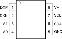
TMP421-Q1 DCN Package
8-Pin SOT-23
Top View

TMP421-Q1 Pin Functions
| PIN | TYPE | DESCRIPTION | |
|---|---|---|---|
| NO. | NAME | ||
| 1 | DXP | Analog input | Positive connection to remote temperature sensor |
| 2 | DXN | Analog input | Negative connection to remote temperature sensor |
| 3 | A1 | Digital input | Address pin |
| 4 | A0 | Digital input | Address pin |
| 5 | GND | Ground | Ground |
| 6 | SDA | Bidirectional digital input-output | Serial data line for SMBus, open-drain; requires pullup resistor to V+ |
| 7 | SCL | Digital input | Serial clock line for SMBus, open-drain; requires pullup resistor to V+ |
| 8 | V+ | Power supply | Positive supply voltage (2.7 V to 5.5 V for the TMP421-Q1) |
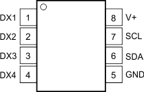
TMP422-Q1 DCN Package
8-Pin SOT-23
Top View

TMP422-Q1 Pin Functions
| PIN | TYPE | DESCRIPTION | |
|---|---|---|---|
| NO. | NAME | ||
| 1 | DX1 | Analog input | Channel 1 remote temperature sensor connection pin. Also sets the TMP422-Q1 address; see Table 4. |
| 2 | DX2 | Analog input | Channel 1 remote temperature sensor connection pin. Also sets the TMP422-Q1 address; see Table 4. |
| 3 | DX3 | Analog input | Channel 2 remote temperature sensor connection pin. Also sets the TMP422-Q1 address; see Table 4. |
| 4 | DX4 | Analog input | Channel 2 remote temperature sensor connection pin. Also sets the TMP422-Q1 address; see Table 4. |
| 5 | GND | Ground | Ground |
| 6 | SDA | Bidirectional digital input-output | Serial data line for SMBus, open-drain; requires pullup resistor to V+. |
| 7 | SCL | Digital input | Serial clock line for SMBus, open-drain; requires pullup resistor to V+. |
| 8 | V+ | Power supply | Positive supply voltage (2.7 V to 5.5 V). |
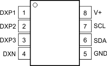
TMP423-Q1 DCN Package
8-Pin SOT-23
Top View

TMP423-Q1 Pin Functions
| PIN | TYPE | DESCRIPTION | |
|---|---|---|---|
| NO. | NAME | ||
| 1 | DXP1 | Analog input | Channel 1 positive connection to remote temperature sensor |
| 2 | DXP2 | Analog input | Channel 2 positive connection to remote temperature sensor |
| 3 | DXP3 | Analog input | Channel 3 positive connection to remote temperature sensor |
| 4 | DXN | Analog input | Common negative connection to remote temperature sensors, channel 1, channel 2, and channel 3 |
| 5 | GND | Ground | Ground |
| 6 | SDA | Bidirectional digital input-output | Serial data line for SMBus, open-drain; requires pullup resistor to V+ |
| 7 | SCL | Digital input | Serial clock line for SMBus, open-drain; requires pullup resistor to V+ |
| 8 | V+ | Power supply | Positive supply voltage (2.7 V to 5.5 V) |