JAJSD83C May 2017 – October 2019 TMP464
PRODUCTION DATA.
- 1 特長
- 2 アプリケーション
- 3 概要
- 4 改訂履歴
- 5 概要(続き)
- 6 Pin Configuration and Functions
- 7 Specifications
-
8 Detailed Description
- 8.1 Overview
- 8.2 Functional Block Diagram
- 8.3 Feature Description
- 8.4 Device Functional Modes
- 8.5 Programming
- 8.6
Register Maps
- 8.6.1
Register Information
- 8.6.1.1 Pointer Register
- 8.6.1.2 Local and Remote Temperature Value Registers
- 8.6.1.3 Software Reset Register
- 8.6.1.4 THERM Status Register
- 8.6.1.5 THERM2 Status Register
- 8.6.1.6 Remote Channel Open Status Register
- 8.6.1.7 Configuration Register
- 8.6.1.8 η-Factor Correction Register
- 8.6.1.9 Remote Temperature Offset Register
- 8.6.1.10 THERM Hysteresis Register
- 8.6.1.11 Local and Remote THERM and THERM2 Limit Registers
- 8.6.1.12 Block Read - Auto Increment Pointer
- 8.6.1.13 Lock Register
- 8.6.1.14 Manufacturer and Device Identification Plus Revision Registers
- 8.6.1
Register Information
- 9 Application and Implementation
- 10Power Supply Recommendations
- 11Layout
- 12デバイスおよびドキュメントのサポート
- 13メカニカル、パッケージ、および注文情報
パッケージ・オプション
メカニカル・データ(パッケージ|ピン)
- RGT|16
サーマルパッド・メカニカル・データ
- RGT|16
発注情報
8.6.1.1 Pointer Register
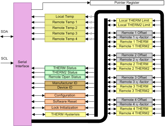
Figure 19 shows the internal register structure of the TMP464 device. The 8-bit pointer register addresses a given data register. The pointer register identifies which of the data registers must respond to a read or write command on the two-wire bus. This register is set with every write command. A write command must be issued to set the proper value in the pointer register before executing a read command. Table 3 describes the pointer register and the internal structure of the TMP464 registers. The power-on-reset (POR) value of the pointer register is 00h (0000 0000b). Table 3 lists a summary of the pointer values for the different registers. Writing data to unassigned pointer values are ignored and does not affect the operation of the device. Reading an unassigned register returns undefined data and is ACKed.
 Figure 19. TMP464 Internal Register Structure