SLOS367E August 2003 – November 2015 TPA6211A1
PRODUCTION DATA.
- 1 Features
- 2 Applications
- 3 Description
- 4 Revision History
- 5 Device Comparison Table
- 6 Pin Configuration and Functions
- 7 Specifications
- 8 Parameter Measurement Information
- 9 Detailed Description
-
10Application and Implementation
- 10.1 Application Information
- 10.2
Typical Application
- 10.2.1 Design Requirements
- 10.2.2 Detailed Design Procedure
- 10.2.3 Application Curves
- 10.3 System Examples
- 11Power Supply Recommendations
- 12Layout
- 13Device and Documentation Support
- 14Mechanical, Packaging, and Orderable Information
パッケージ・オプション
デバイスごとのパッケージ図は、PDF版データシートをご参照ください。
メカニカル・データ(パッケージ|ピン)
- DGN|8
- DRB|8
サーマルパッド・メカニカル・データ
発注情報
10 Application and Implementation
NOTE
Information in the following applications sections is not part of the TI component specification, and TI does not warrant its accuracy or completeness. TI’s customers are responsible for determining suitability of components for their purposes. Customers should validate and test their design implementation to confirm system functionality.
10.1 Application Information
The TPA6211A1 is a fully-differential amplifier designed to drive a speaker with at least 3-Ω impedance while consuming only 20 mm2 total printed circuit board (PCB) area in most applications.
10.2 Typical Application
Figure 31 shows a typical application circuit for the TPA6211A1 with a speaker, input resistors and supporting power supply decoupling capacitors.
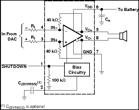 Figure 31. Typical Differential Input Application Schematic
Typical values are shown in Table 3.
Table 3. Typical Component Values
| COMPONENT | VALUE |
|---|---|
| RI | 40 kΩ |
| C(BYPASS)(1) | 0.22 μF |
| CS | 1 μF |
| CI | 0.22 μF |
10.2.1 Design Requirements
For this design example, use the parameters listed in Table 4.
Table 4. Design Parameters
| DESIGN PARAMETER | EXAMPLE VALUE |
|---|---|
| Power supply | 2.5 V to 5.5 V |
| Current | 4 mA to 5 mA |
| Shutdown | High > 1.55 V |
| Low < 0.5 V | |
| Speaker | 3 Ω, 4 Ω, or 8 Ω |
10.2.2 Detailed Design Procedure
10.2.2.1 Selecting Components
10.2.2.1.1 Resistors (RI)
The input resistor (RI) can be selected to set the gain of the amplifier according to Equation 9.

The internal feedback resistors (RF) are trimmed to 40 kΩ.
Resistor matching is very important in fully differential amplifiers. The balance of the output on the reference voltage depends on matched ratios of the resistors. CMRR, PSRR, and the cancellation of the second harmonic distortion diminishes if resistor mismatch occurs. Therefore, 1%-tolerance resistors or better are recommended to optimize performance.
10.2.2.1.2 Bypass Capacitor (CBYPASS) and Start-Up Time
The internal voltage divider at the BYPASS pin of this device sets a mid-supply voltage for internal references and sets the output common mode voltage to VDD/2. Adding a capacitor filters any noise into this pin, increasing kSVR. C(BYPASS)also determines the rise time of VO+ and VO- when the device exits shutdown. The larger the capacitor, the slower the rise time.
10.2.2.1.3 Input Capacitor (CI)
The TPA6211A1 does not require input coupling capacitors when driven by a differential input source biased from 0.5 V to VDD - 0.8 V. Use 1% tolerance or better gain-setting resistors if not using input coupling capacitors.
In the single-ended input application, an input capacitor, CI, is required to allow the amplifier to bias the input signal to the proper dc level. In this case, CI and RI form a high-pass filter with the corner frequency defined in Equation 10.

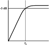 Figure 32. Input Filter Cutoff Frequency
The value of CI is an important consideration. It directly affects the bass (low frequency) performance of the circuit. Consider the example where RI is 10 kΩ and the specification calls for a flat bass response down to 100 Hz. Equation 10 is reconfigured as Equation 11.

In this example, CI is 0.16 μF, so the likely choice ranges from 0.22 μF to 0.47 μF. Ceramic capacitors are preferred because they are the best choice in preventing leakage current. When polarized capacitors are used, the positive side of the capacitor faces the amplifier input in most applications. The input dc level is held at VDD/2, typically higher than the source dc level. It is important to confirm the capacitor polarity in the application.
10.2.2.1.4 Band-Pass Filter (Ra, Ca, and Ca)
It may be desirable to have signal filtering beyond the one-pole high-pass filter formed by the combination of CI and RI. A low-pass filter may be added by placing a capacitor (CF) between the inputs and outputs, forming a band-pass filter.
An example of when this technique might be used would be in an application where the desirable pass-band range is between 100 Hz and 10 kHz, with a gain of 4 V/V. The following equations illustrate how the proper values of CF and CI can be determined.
10.2.2.1.4.1 Step 1: Low-Pass Filter

where
- RF is the internal 40 kΩ resistor

Therefore,

Substitute fc(LPF) with 10 kHz and solve for CF: CF = 398 pF
10.2.2.1.4.2 Step 2: High-Pass Filter

where
- R| is the input resistor
Because the application in this case requires a gain of 4 V/V, RI must be set to 10 kΩ.
Substitute RI in Equation 15 with 10 kΩ as shown in Equation 16.

Therefore,

Substitute fc(HPF) with 100 Hz and solve for CI: CI = 0.16 μF
At this point, a first-order band-pass filter has been created with the low-frequency cutoff set to 100 Hz and the high-frequency cutoff set to 10 kHz.
The process can be taken a step further by creating a second-order high-pass filter. This is accomplished by placing a resistor (Ra) and capacitor (Ca) in the input path. It is important to note that Ra must be at least 10 times smaller than RI; otherwise its value has a noticeable effect on the gain, as Ra and RI are in series.
10.2.2.1.4.3 Step 3: Additional Low-Pass Filter
Ra must be at least 10x smaller than RI, Set Ra = 1 kΩ,

Therefore,

Substitute fc(LPF) with 10 kHz and solving for Ca: Ca = 160 pF
Figure 33 is a bode plot for the band-pass filter in the previous example. Figure 38 shows how to configure the TPA6211A1 as a band-pass filter.
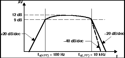 Figure 33. Bode Plot
10.2.2.1.5 Decoupling Capacitor (CS)
The TPA6211A1 is a high-performance CMOS audio amplifier that requires adequate power supply decoupling to ensure the output total harmonic distortion (THD) is as low as possible. Power-supply decoupling also prevents oscillations for long lead lengths between the amplifier and the speaker. For higher frequency transients, spikes, or digital hash on the line, a good low equivalent-series-resistance (ESR) ceramic capacitor, typically 0.1 μF to 1 μF, placed as close as possible to the device VDD lead works best. For filtering lower frequency noise signals, a 10-μF or greater capacitor placed near the audio power amplifier also helps, but is not required in most applications because of the high PSRR of this device.
10.2.2.1.6 Using Low-ESR Capacitors
Low-ESR capacitors are recommended throughout this application section. A real (as opposed to ideal) capacitor can be modeled simply as a resistor in series with an ideal capacitor. The voltage drop across this resistor minimizes the beneficial effects of the capacitor in the circuit. The lower the equivalent value of this resistance the more the real capacitor behaves like an ideal capacitor.
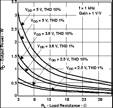
10.2.3 Application Curves
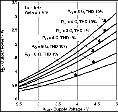
10.3 System Examples
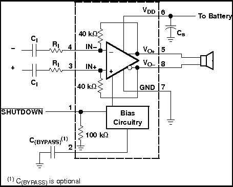 Figure 36. Differential Input Application Schematic Optimized With Input Capacitors
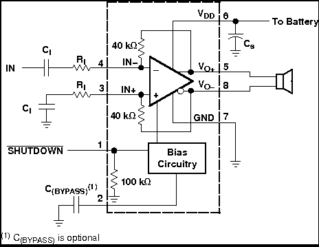 Figure 37. Single-Ended Input Application Schematic
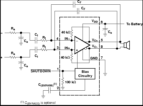 Figure 38. Differential Input Application Schematic With Input Bandpass Filter