SLOS367E August   2003  – November 2015 TPA6211A1

PRODUCTION DATA.  

  1. Features
  2. Applications
  3. Description
  4. Revision History
  5. Device Comparison Table
  6. Pin Configuration and Functions
  7. Specifications
    1. 7.1 Absolute Maximum Ratings
    2. 7.2 ESD Ratings
    3. 7.3 Recommended Operation Conditions
    4. 7.4 Thermal Information
    5. 7.5 Electrical Characteristics
    6. 7.6 Operating Characteristics
    7. 7.7 Dissipation Ratings
    8. 7.8 Typical Characteristics
  8. Parameter Measurement Information
  9. Detailed Description
    1. 9.1 Overview
    2. 9.2 Functional Block Diagram
    3. 9.3 Feature Description
      1. 9.3.1 Fully Differential Amplifier Efficiency and Thermal Information
        1. 9.3.1.1 Advantages of Fully Differential Amplifiers
        2. 9.3.1.2 Differential Output Versus Single-Ended Output
    4. 9.4 Device Functional Modes
      1. 9.4.1 Shutdown Mode
  10. 10Application and Implementation
    1. 10.1 Application Information
    2. 10.2 Typical Application
      1. 10.2.1 Design Requirements
      2. 10.2.2 Detailed Design Procedure
        1. 10.2.2.1 Selecting Components
          1. 10.2.2.1.1 Resistors (RI)
          2. 10.2.2.1.2 Bypass Capacitor (CBYPASS) and Start-Up Time
          3. 10.2.2.1.3 Input Capacitor (CI)
          4. 10.2.2.1.4 Band-Pass Filter (Ra, Ca, and Ca)
            1. 10.2.2.1.4.1 Step 1: Low-Pass Filter
            2. 10.2.2.1.4.2 Step 2: High-Pass Filter
            3. 10.2.2.1.4.3 Step 3: Additional Low-Pass Filter
          5. 10.2.2.1.5 Decoupling Capacitor (CS)
          6. 10.2.2.1.6 Using Low-ESR Capacitors
      3. 10.2.3 Application Curves
    3. 10.3 System Examples
  11. 11Power Supply Recommendations
    1. 11.1 Power Supply Decoupling Capacitor
  12. 12Layout
    1. 12.1 Layout Guidelines
    2. 12.2 Layout Examples
  13. 13Device and Documentation Support
    1. 13.1 Device Support
      1. 13.1.1 Development Support
    2. 13.2 Documentation Support
      1. 13.2.1 Related Documentation
    3. 13.3 Community Resources
    4. 13.4 Trademarks
    5. 13.5 Electrostatic Discharge Caution
    6. 13.6 Glossary
  14. 14Mechanical, Packaging, and Orderable Information

パッケージ・オプション

デバイスごとのパッケージ図は、PDF版データシートをご参照ください。

メカニカル・データ(パッケージ|ピン)
  • DGN|8
  • DRB|8
サーマルパッド・メカニカル・データ
発注情報

12 Layout

12.1 Layout Guidelines

Place all the external components close to the TPA6211A1 device. The input resistors need to be close to the device input pins so noise does not couple on the high impedance nodes between the input resistors and the input amplifier of the device. Placing the decoupling capacitors, CS and C(BYPASS), close to the TPA6211A1 device is important for the efficiency of the amplifier. Any resistance or inductance in the trace between the device and the capacitor can cause a loss in efficiency.

12.2 Layout Examples
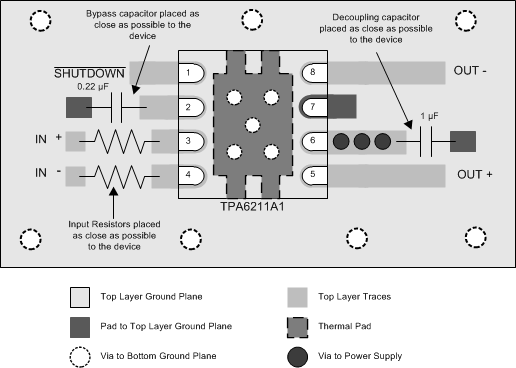
TPA6211A1 tpa6211a1_son_layout.gif Figure 39. TPA6211A1 8-Pin SON (DRB) Board Layout
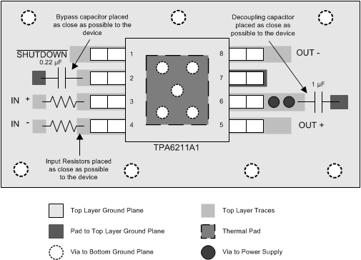
TPA6211A1 tpa6211a1_msop_layout.gif Figure 40. TPA6211A1 8-Pin MSOP-PowerPAD™ (DGN) Board Layout