JAJSDV1A June 2017 – September 2017 TPD4E02B04-Q1
PRODUCTION DATA.
- 1 特長
- 2 アプリケーション
- 3 概要
- 4 改訂履歴
- 5 Pin Configuration and Functions
- 6 Specifications
-
7 Detailed Description
- 7.1 Overview
- 7.2 Functional Block Diagram
- 7.3
Feature Description
- 7.3.1 AEC-Q101 Qualified
- 7.3.2 ISO 10605 ESD Protection
- 7.3.3 IEC 61000-4-2 ESD Protection
- 7.3.4 IEC 61000-4-4 EFT Protection
- 7.3.5 IEC 61000-4-5 Surge Protection
- 7.3.6 IO Capacitance
- 7.3.7 DC Breakdown Voltage
- 7.3.8 Ultra Low Leakage Current
- 7.3.9 Low ESD Clamping Voltage
- 7.3.10 Supports High Speed Interfaces
- 7.3.11 Industrial Temperature Range
- 7.3.12 Easy Flow-Through Routing Package
- 7.4 Device Functional Modes
- 8 Application and Implementation
- 9 Power Supply Recommendations
- 10Layout
- 11デバイスおよびドキュメントのサポート
- 12メカニカル、パッケージ、および注文情報
パッケージ・オプション
メカニカル・データ(パッケージ|ピン)
- DQA|10
サーマルパッド・メカニカル・データ
- DQA|10
発注情報
8 Application and Implementation
NOTE
Information in the following applications sections is not part of the TI component specification, and TI does not warrant its accuracy or completeness. TI’s customers are responsible for determining suitability of components for their purposes. Customers should validate and test their design implementation to confirm system functionality.
8.1 Application Information
The TPD4E02B04-Q1 is a diode type TVS which is used to provide a path to ground for dissipating ESD events on high-speed signal lines between a human interface connector and a system. As the current from ESD passes through the TVS, only a small voltage drop is present across the diode. This is the voltage presented to the protected IC. The low RDYN of the triggered TVS holds this voltage, VCLAMP, to a safe level for the protected IC.
8.2 Typical Application
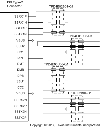
 Figure 20. USB 3.1 Gen 2 Type-C ESD Schematic
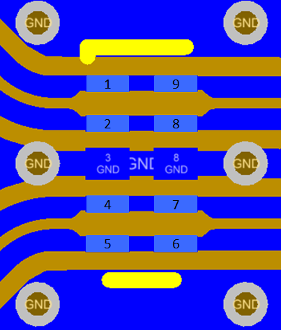
 Figure 21. USB 3.1 Gen 2 SuperSpeed Layout
8.2.1 Design Requirements
For this design example two TPD4E02B04-Q1 devices and two TPD4E05U06 devices are being used in a USB 3.1 Gen 2 Type-C application. This provides a complete ESD protection scheme.
Given the USB 3.1 Gen 2 Type-C application, the parameters listed in Table 1 are known.
Table 1. Design Parameters
| DESIGN PARAMETER | VALUE |
|---|---|
| Signal Range on SuperSpeed+ Lines | 0 V to 3.6 V |
| Operating Frequency on SuperSpeed+ Lines | 5 GHz |
| Signal Range on CC, SBU, and DP/DM Lines | 0 V to 5 V |
| Operating Frequency on CC, SBU, and DP/DM Lines | up to 480 MHz |
8.2.2 Detailed Design Procedure
8.2.2.1 Signal Range
The TPD4E02B04-Q1 supports signal ranges between –3.6 V and 3.6 V, which supports the SuperSpeed+ pairs on the USB Type-C application. The TPD4E05U06 supports signal ranges between 0 V and 5.5 V, which supports the CC, SBU, and DP/DM lines.
8.2.2.2 Operating Frequency
The TPD4E02B04-Q1 has a 0.25 pF (typical) capacitance, which supports the USB3.1 Gen 2 data rates of 10 Gbps. The TPD4E05U06 has a 0.5 pF (typical) capacitance, which easily supports the CC, SBU, and DP/DM data rates.
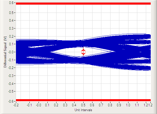
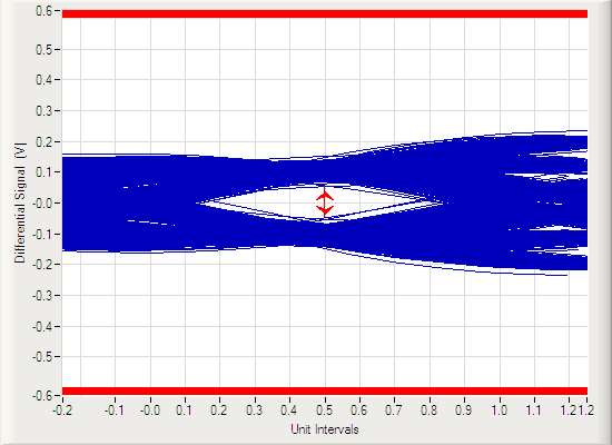
8.2.3 Application Curves

