SLVSCK3C May 2014 – February 2017 TPD4E6B06
PRODUCTION DATA.
- 1 Features
- 2 Applications
- 3 Description
- 4 Revision History
- 5 Pin Configuration and Functions
- 6 Specifications
- 7 Detailed Description
- 8 Application and Implementation
- 9 Power Supply Recommendations
- 10Layout
- 11Device and Documentation Support
- 12Mechanical, Packaging, and Orderable Information
パッケージ・オプション
メカニカル・データ(パッケージ|ピン)
- DPW|4
サーマルパッド・メカニカル・データ
- DPW|4
発注情報
8 Application and Implementation
NOTE
Information in the following applications sections is not part of the TI component specification, and TI does not warrant its accuracy or completeness. TI’s customers are responsible for determining suitability of components for their purposes. Customers should validate and test their design implementation to confirm system functionality.
8.1 Application Information
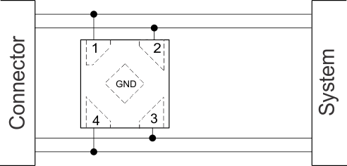
The TPD4E6B06 is a diode array type TVS. These low capacitance types of TVSs are typically used to provide a path to ground for dissipating ESD events on hi speed signal lines between a human interface connector and a system. During high voltage ESD strikes, the device clamps to a safe voltage level to protect the system.
The typical application of the TPD4E6B06 is to be placed in between the connector and the system. The low capacitance of the TPD4E6B06 gives flexibility in the end application, as it can be used on many different high speed interfaces.
8.2 Typical Application
 Figure 10. Protecting Data Lines
8.2.1 Design Requirements
Table 1 shows the design parameters.
Table 1. Design Parameters
| DESIGN PARAMETER | EXAMPLE VALUE |
|---|---|
| Signal range on data lines | –5.5 V to 5.5 V |
| Operating frequency | Up to 700 MHz |
8.2.2 Detailed Design Procedure
The designer needs to know the following:
- Signal range on all the protected lines
- Operating frequency
8.2.2.1 Signal Range
The TPD4E6B06 has 4 protection channels for signal lines. Any I/O supports a signal range of –5.5 V to
5.5 V.
8.2.2.2 Operating Frequency
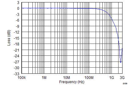
The TPD4E6B06 has 4.8 pF of capacitance (Typical), supporting up to 700 MHz frequencies.
8.2.3 Application Curve
 Figure 11. Insertion Loss (Any IO to GND)