SLVSCK3C May 2014 – February 2017 TPD4E6B06
PRODUCTION DATA.
- 1 Features
- 2 Applications
- 3 Description
- 4 Revision History
- 5 Pin Configuration and Functions
- 6 Specifications
- 7 Detailed Description
- 8 Application and Implementation
- 9 Power Supply Recommendations
- 10Layout
- 11Device and Documentation Support
- 12Mechanical, Packaging, and Orderable Information
パッケージ・オプション
メカニカル・データ(パッケージ|ピン)
- DPW|4
サーマルパッド・メカニカル・データ
- DPW|4
発注情報
7 Detailed Description
7.1 Overview
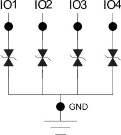
The TPD4E6B06 is a four channel ESD Protection device in an ultra small DPW package. It is the industry’s smallest 4-CH ESD protection device with 0.48-mm pitch. This larger pitch helps save on PCB manufacturing costs. The device provides IEC61000-4-2 compliance up to 15-kV contact discharge. It has an ESD clamp circuit with back-to-back diodes for bipolar/bidirectional signal support. The 4.8-pF (Typical) line capacitance is suitable for a wide range of applications supporting frequencies up to 700 MHz.
7.2 Functional Block Diagram

7.3 Feature Description
7.3.1 IEC 61000-4-2 Level 2 ESD Protection
The IO pins can withstand ESD events up to ±15-kV contact and ±15-kV air. An ESD-surge clamp diverts the current to ground.
7.3.2 IEC 61000-4-5 Surge Protection
The IO pins can withstand surge events up to 3 A and 40 W (8/20 µs waveform). An ESD-surge clamp diverts this current to ground.
7.3.3 IO Capacitance
The capacitance between any IO pin to ground is 4.8 pF (typical). This capacitance supports frequencies up to 700 MHz.
7.3.4 RDYN
The low RDYN of 0.75 Ω (typical) allows for lower clamping voltages.
7.3.5 DC Breakdown Voltage
The DC breakdown voltage of any IO pin is a minimum of ±6 V. This ensures that sensitive equipment is protected from surges above the reverse standoff voltage of ±5.5 V (minimum).
7.3.6 Ultra-Low Leakage Current
The IO pins feature an ultra-low leakage current of 100 nA (maximum) with a bias of 2.5 V.
7.3.7 Clamping Voltage
The IO pins feature an ESD clamp capable of clamping the voltage to 10 V (IO to GND) or 9 V (GND to IO) of IEC61000-4-5 surge when IPP = 1 A.
7.3.8 Industrial Temperature Range
This device features an industrial operating range of –40°C to +125°C.
7.3.9 Space Saving DPW Package
The small 0.8 mm × 0.8 mm package size saves board space and makes it easy to add ESD protection.
7.4 Device Functional Modes
The TPD4E6B06 is a passive integrated circuit that triggers when voltages are above VBRF or VBRR. During ESD events, voltages as high as ±15 kV (air) can be directed to ground via the internal diode network. Once the voltages on the protected line fall below the trigger levels of the TPD4E6B06 (usually within 10s of nano-seconds) the device reverts to passive.