SLVS928B March 2009 – August 2014 TPD4S012
UNLESS OTHERWISE NOTED, this document contains PRODUCTION DATA.
- 1 Features
- 2 Applications
- 3 Description
- 4 Revision History
- 5 Pin Configurations and Functions
- 6 Specifications
- 7 Detailed Description
- 8 Applications and Implementation
- 9 Power Supply Recommendations
- 10Layout
- 11Device and Documentation Support
- 12Mechanical, Packaging, and Orderable Information
パッケージ・オプション
メカニカル・データ(パッケージ|ピン)
- DRY|6
サーマルパッド・メカニカル・データ
- DRY|6
発注情報
7 Detailed Description
7.1 Overview
The TPD4S012 is a four-channel Transient Voltage Suppressor (TVS) based Electrostatic Discharge (ESD) protection diode array for USB chargers and USB On-The-Go (OTG) interfaces.
The TPD4S012 provides IEC 61000-4-2 system level ESD Protection featuring 15 V tolerance on the VBUS line. The device is ideal for providing circuit protection for USB charger and OTG applications due to its high-voltage tolerance at the VBUS line and small flow-through package.
7.2 Functional Block Diagram
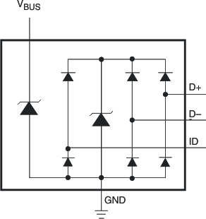
7.3 Feature Description
7.3.1 Integrated ESD Clamps
Integrated ESD Clamps on the D+, D–, VBUS, and ID pins provide single-chip ESD protection for USB High Speed, USB-OTG, and USB charger interfaces.
7.3.2 USB Signal Pins
D+, D– and ID USB Signal pins have low capacitance (0.8 pF Typ).
7.3.3 VBUS Line
The VBUS line has a 11 pF (Typ) capacitance.
7.3.4 Supports Data Rates in Excess of 480 Mbps
The low capacitance (0.8 pF Typ) of the data lines supports speeds in excess of 480 Mbps.
7.3.5 IEC 61000-4-2 (Level 4 Contact)
IEC 61000-4-2 (Level 4 contact) system level ESD compliance measured at the D+, D– and ID pins is rated for ±10 kV contact and air-gap discharge.
7.3.6 IEC 61000-4-5 Surge
IEC 61000-4-5 system level surge compliance measured at D+, D–, ID, and VBUS pins rated to 3 A of peak pulse current.
7.4 Device Functional Modes
The TPD4S012 is a passive integrated circuit that triggers when voltages are above VBR or below the lower diode's Vf. During ESD events, voltages as high as ±10 kV (contact) can be directed to ground via the internal diode network. Once the voltages on the protected line fall below the trigger levels of TPD4S012 (usually within 10's of nano-seconds), the device reverts to passive.