SLVS928B March 2009 – August 2014 TPD4S012
UNLESS OTHERWISE NOTED, this document contains PRODUCTION DATA.
- 1 Features
- 2 Applications
- 3 Description
- 4 Revision History
- 5 Pin Configurations and Functions
- 6 Specifications
- 7 Detailed Description
- 8 Applications and Implementation
- 9 Power Supply Recommendations
- 10Layout
- 11Device and Documentation Support
- 12Mechanical, Packaging, and Orderable Information
パッケージ・オプション
メカニカル・データ(パッケージ|ピン)
- DRY|6
サーマルパッド・メカニカル・データ
- DRY|6
発注情報
10 Layout
10.1 Layout Guidelines
- The optimum placement is as close to the connector as possible.
- EMI during an ESD event can couple from the trace being struck to other nearby unprotected traces, resulting in early system failures.
- The PCB designer needs to minimize the possibility of EMI coupling by keeping any unprotected traces away from the protected traces which are between the TVS and the connector.
- Route the protected traces as straight as possible.
- Eliminate any sharp corners on the protected traces between the TVS and the connector by using rounded corners with the largest radii possible.
- Electric fields tend to build up on corners, increasing EMI coupling.
10.2 Layout Example
This application is typical of a mobile USB platform with an ID pin in addition to the D+, D–, and VBUS pins.
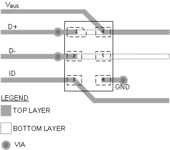 Figure 16. Using DRY Package