SLVS928B March 2009 – August 2014 TPD4S012
UNLESS OTHERWISE NOTED, this document contains PRODUCTION DATA.
- 1 Features
- 2 Applications
- 3 Description
- 4 Revision History
- 5 Pin Configurations and Functions
- 6 Specifications
- 7 Detailed Description
- 8 Applications and Implementation
- 9 Power Supply Recommendations
- 10Layout
- 11Device and Documentation Support
- 12Mechanical, Packaging, and Orderable Information
パッケージ・オプション
メカニカル・データ(パッケージ|ピン)
- DRY|6
サーマルパッド・メカニカル・データ
- DRY|6
発注情報
6 Specifications
6.1 Absolute Maximum Ratings
Over operating free-air temperature range (unless otherwise noted)| PARAMETER | MIN | MAX | UNIT | |||
|---|---|---|---|---|---|---|
| VBUS voltage tolerance | VBUS pin | –0.3 | 20 | V | ||
| IO voltage tolerance | D+, D–, ID pins | –0.3 | 6 | V | ||
| TA | Operating free-air temperature range | –40 | 85 | °C | ||
| IEC 61000-4-2 Contact Discharge | D+, D–, ID | ±10 | kV | |||
| VBUS pin | ±10 | kV | ||||
| IEC 61000-4-2 Air-Gap Discharge | D+, D–, ID | ±10 | kV | |||
| VBUS pin | ±9 | kV | ||||
| IEC 61000-4-5 Surge (tp = 8/20 μs) | Peak pulse Power (All pins) | 60 | W | |||
| Peak pulse current (All Pins) | 3 | A | ||||
6.2 Handling Ratings
| MIN | MAX | UNIT | |||
|---|---|---|---|---|---|
| Tstg | Storage temperature range | –65 | 125 | °C | |
| V(ESD) | Electrostatic discharge | Human body model (HBM), per ANSI/ESDA/JEDEC JS-001, all pins(1) | –2.5 | 2.5 | kV |
| Charged device model (CDM), per JEDEC specification JESD22-C101, all pins(2) | –1 | 1 | |||
(1) JEDEC document JEP155 states that 500-V HBM allows safe manufacturing with a standard ESD control process.
(2) JEDEC document JEP157 states that 250-V CDM allows safe manufacturing with a standard ESD control process.
6.3 Recommended Operating Conditions
over operating free-air temperature range (unless otherwise noted)| PARAMETER | MIN | MAX | UNIT | |
|---|---|---|---|---|
| TA Operating free-air Temperature Range | –40 | 85 | °C | |
| Operating Voltage | VBUS Pin | 0 | 15 | V |
| D+, D–, ID Pins | 0 | 5.5 | ||
6.4 Thermal Information
| THERMAL METRIC(1) | TPD4S012 | UNIT | |
|---|---|---|---|
| DRY | |||
| 6 PINS | |||
| RθJA | Junction-to-ambient thermal resistance | 461.3 | °C/W |
| RθJC(top) | Junction-to-case (top) thermal resistance | 219.6 | |
| RθJB | Junction-to-board thermal resistance | 343.7 | |
| ψJT | Junction-to-top characterization parameter | 162.5 | |
| ψJB | Junction-to-board characterization parameter | 343.7 | |
(1) For more information about traditional and new thermal metrics, see the IC Package Thermal Metrics application report, SPRA953.
6.5 Electrical Characteristics
over operating free-air temperature range (unless otherwise noted)| PARAMETER | TEST CONDITIONS | MIN | TYP | MAX | UNIT | ||||
|---|---|---|---|---|---|---|---|---|---|
| IVBUS | VBUS operating current | VBUS = 19 V | D+, D–, ID pins open | 0.1 | 0.5 | μA | |||
| IIO | IO port current | VIO = 2.5 V, VBUS = 5 V | D+, D–, ID pins | 0.1 | 0.5 | μA | |||
| VD | Diode forward voltage | IIO = 8 mA | D+, D–, ID pins (lower clamp diode) | 0.6 | 0.8 | 0.95 | V | ||
| CVBUS | VBUS pin capacitance | VBUS = 5 V | 11 | 15 | pF | ||||
| CIO | IO capacitance | VIO = 2.5 V | D+, D–, ID pins | 0.8 | 1 | pF | |||
| RDYN | Dynamic resistance | IIO = 1.5 A | D+, D–, ID, and VBUS pins, including central clamp dioded during positive ESD pulse | 1.2 | Ω | ||||
| IIO = 1 A | D+, D–, ID, and VBUS pins, including central clamp diode during negative ESD pulse | 1 | |||||||
| VBR | Breakdown voltage | IIO = 1 mA | D+, D–, ID pins | 6 | 9 | V | |||
| VBUS pin(s) | 20 | 24 | |||||||
6.6 Typical Characteristics
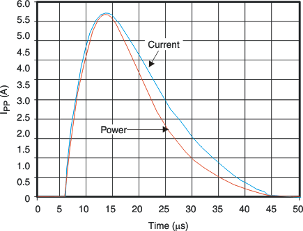 Figure 1. Peak Pulse Power Waveform at the D+, D–, or ID Pin
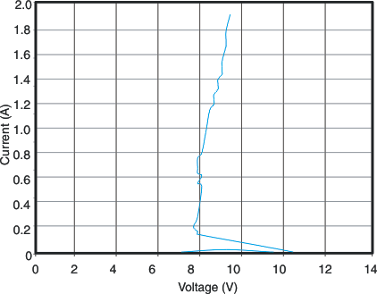 Figure 3. D+, D–, or ID Clamp Voltage Under ESD Event
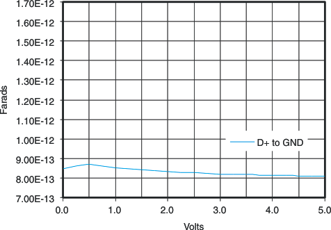 Figure 5. D+, D–, or ID Capacitance, TA = 27°C
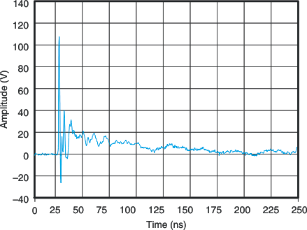 Figure 7. IEC Clamping Waveform, 8 kV Contact, D+, 25 ns/div
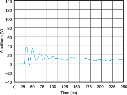 Figure 9. VBUS IEC Clamping Waveform, 8 kV Contact, 25 ns/div
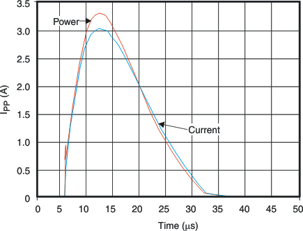 Figure 2. Peak Pulse Power Waveform at the VBUS Pin
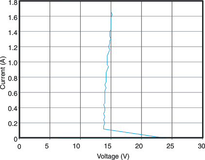 Figure 4. VBUS Clamp Voltage Under ESD Event
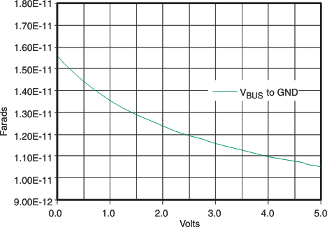 Figure 6. VBUS Capacitance, TA = 27°C
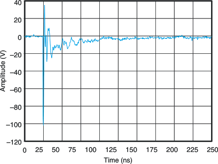 Figure 8. IEC Clamping Waveform, –8 kV Contact, D+, 25 ns/div
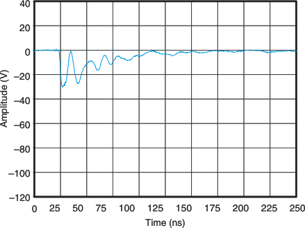 Figure 10. VBUS IEC Clamping Waveform, –8 kV Contact, 25 ns/div