JAJSG28F august   2018  – august 2020 TPS2120 , TPS2121

PRODUCTION DATA  

  1.   1
  2. 特長
  3. アプリケーション
  4. 概要
  5. Revision History
  6. Device Comparison Table
  7. Pin Configuration and Functions
    1.     8
  8. Specifications
    1. 7.1 Absolute Maximum Ratings
    2. 7.2 ESD Ratings
    3. 7.3 Recommended Operating Conditions
    4. 7.4 Thermal Information
    5. 7.5 Electrical Characteristics
    6. 7.6 Typical Characteristics
  9. Parameter Measurement Information
  10. Detailed Description
    1. 9.1 Overview
    2. 9.2 Functional Block Diagram
    3. 9.3 Feature Description
      1. 9.3.1 Input Settling Time and Output Soft Start Control (SS)
        1. 9.3.1.1 Slew Rate vs. CSS Capacitor
      2. 9.3.2 Active Current Limiting (ILM)
      3. 9.3.3 Short-Circuit Protection
      4. 9.3.4 Thermal Protection (TSD)
      5. 9.3.5 Overvoltage Protection (OVx)
      6. 9.3.6 Fast Reverse Current Blocking (RCB)
      7. 9.3.7 Output Voltage Dip and Fast Switchover Control (TPS2121 only)
      8. 9.3.8 Input Voltage Comparator (VCOMP)
    4. 9.4 TPS2120 Device Functional Modes
    5. 9.5 TPS2121 Device Functional Modes
  11. 10Application and Implementation
    1. 10.1 Application Information
    2. 10.2 Typical Application
      1. 10.2.1 Manual Switchover Schematic
      2. 10.2.2 Design Requirements
      3. 10.2.3 Detailed Design Description
      4. 10.2.4 Design Procedure
        1. 10.2.4.1 Selecting PR1 and CP2 Resistors
        2. 10.2.4.2 Selecting OVx Resistors
        3. 10.2.4.3 Selecting Soft-Start Capacitor and Current Limit Resistors
      5. 10.2.5 Application Curves
    3. 10.3 Automatic Switchover with Priority (XCOMP)
      1. 10.3.1 Application Schematic
      2. 10.3.2 Design Requirements
      3. 10.3.3 Detailed Design Description
      4. 10.3.4 Design Procedure
        1. 10.3.4.1 Selecting PR1 and CP2 Resistors
      5. 10.3.5 Application Curves
    4. 10.4 Automatic Seamless Switchover with Priority (XREF)
      1. 10.4.1 Application Schematic
      2. 10.4.2 Design Requirements
      3. 10.4.3 Detailed Design Description
      4. 10.4.4 Application Curves
    5. 10.5 Highest Voltage Operation (VCOMP)
      1. 10.5.1 Application Schematic
      2. 10.5.2 Design Requirements
      3. 10.5.3 Detailed Design Description
      4. 10.5.4 Detailed Design Procedure
      5. 10.5.5 Application Curves
    6. 10.6 Reverse Polarity Protection with TPS212x
    7. 10.7 Hotplugging with TPS212x
  12. 11Power Supply Recommendations
  13. 12Layout
    1. 12.1 Layout Guidelines
    2. 12.2 Layout Example
  14. 13Device and Documentation Support
    1. 13.1 Documentation Support
      1. 13.1.1 Related Links
    2. 13.2 ドキュメントの更新通知を受け取る方法
    3. 13.3 サポート・リソース
    4. 13.4 Trademarks
    5. 13.5 静電気放電に関する注意事項
    6. 13.6 用語集
  15. 14Mechanical, Packaging, and Orderable Information

パッケージ・オプション

デバイスごとのパッケージ図は、PDF版データシートをご参照ください。

メカニカル・データ(パッケージ|ピン)
  • YFP|20
サーマルパッド・メカニカル・データ
発注情報

Selecting Soft-Start Capacitor and Current Limit Resistors

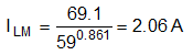
Equation 1 can be used to determine the RLIM values for this application. In this example, the DC load current is 1 A. Setting the current limit to 2 A will limit potential inrush current events and protect downstream loads. See Equation 8 for the TPS2120 ILM Calculation:

Equation 8. GUID-DBD471B6-EC78-484B-BF49-2E7203E6ED70-low.gif

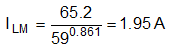
See Equation 9 for the TPS2121 ILM Calculation:

Equation 9. GUID-C4791F4F-2A1D-48F0-894E-9AAA1CD72FDC-low.gif

To calculate the slew rate needed to limit the inrush current to 100 mA, the Slew Rate Calculation can be used in Equation 10:

Equation 10. GUID-214B4519-F340-4BAE-83B4-AC40F75DE20A-low.gif
Equation 11. GUID-AD3F9B1F-21B1-478D-9687-6BB13E39E437-low.gif

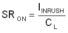
Using this equation, the slew rate must be limited to 1000V/S or below to keep the inrush current below 100 mA. According to Table 9-1, at 5 V a CSS capacitance of 100 nF will provide a slew rate of 780V/S (typical), which is below the calculated threshold of 1000V/S. Therefore, a 100 nF capacitor will limit the inrush below 100 mA in a typical application.