JAJSG28F august 2018 – august 2020 TPS2120 , TPS2121
PRODUCTION DATA
- 1
- 1 特長
- 2 アプリケーション
- 3 概要
- 4 Revision History
- 5 Device Comparison Table
- 6 Pin Configuration and Functions
- 7 Specifications
- 8 Parameter Measurement Information
-
9 Detailed Description
- 9.1 Overview
- 9.2 Functional Block Diagram
- 9.3
Feature Description
- 9.3.1 Input Settling Time and Output Soft Start Control (SS)
- 9.3.2 Active Current Limiting (ILM)
- 9.3.3 Short-Circuit Protection
- 9.3.4 Thermal Protection (TSD)
- 9.3.5 Overvoltage Protection (OVx)
- 9.3.6 Fast Reverse Current Blocking (RCB)
- 9.3.7 Output Voltage Dip and Fast Switchover Control (TPS2121 only)
- 9.3.8 Input Voltage Comparator (VCOMP)
- 9.4 TPS2120 Device Functional Modes
- 9.5 TPS2121 Device Functional Modes
- 10Application and Implementation
- 11Power Supply Recommendations
- 12Layout
- 13Device and Documentation Support
- 14Mechanical, Packaging, and Orderable Information
パッケージ・オプション
デバイスごとのパッケージ図は、PDF版データシートをご参照ください。
メカニカル・データ(パッケージ|ピン)
- YFP|20
サーマルパッド・メカニカル・データ
発注情報
10.2.3 Detailed Design Description
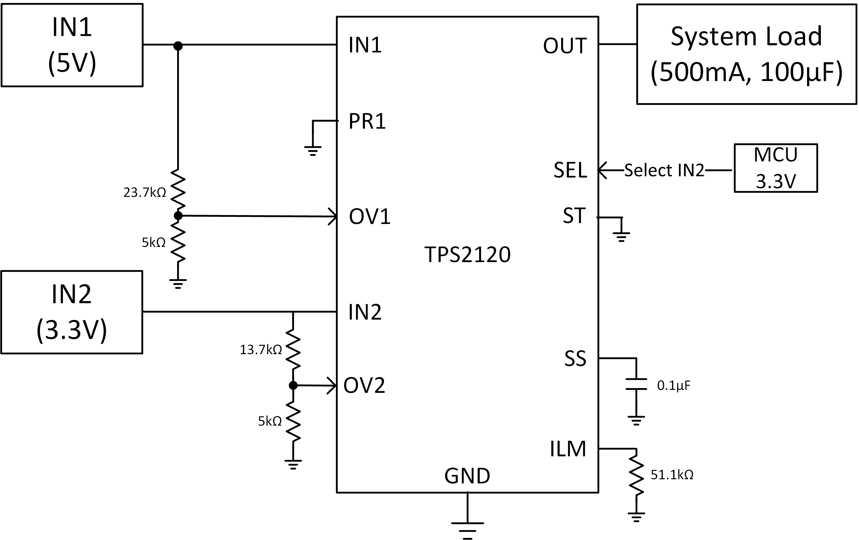
The TPS212x devices can be configured to manually switch between IN1 and IN2 through an external GPIO. In this example, an external MCU signal is selecting between main power and auxiliary power to power a downstream load. By manually toggling the TPS212x, the device will switch between both sources, even if one supply is higher than the other supply. Ultimately, the main factor that will determine the switchover time between IN1 (5 V) and IN2 (3.3 V) is the output load.
Manual switchover can be enabled by configuring the TPS212x for internal voltage reference control scheme (VREF). In the VREF scheme, if the voltage on PR1 is higher than the internal VREF voltage, 1.06 V (typical), the device will select IN1 as the output. If the voltage on PR1 drops below VREF, then the device will switch to IN2, as long as IN2 is presenting a valid input voltage. IN1 is commonly connected to PR1 with an external resistor divider. OV1 and OV2 can be configured to provide overvoltage protection. The ST pin can be pulled high with a resistor to provide feedback on the status of the system. If the status pin is high, IN1 is the output. If the pin is low, IN2 is the output. If this feature is not required, the ST pin can be connected to GND.
On the TPS2120, by connecting an external signal to the select pin (SEL), the device can override the PR1/VREF comparison. If the voltage on SEL is higher than VREF at approximately (1.06 V), then the device will select IN2, as shown on Table 9-2. If the voltage on SEL drops below VREF, then the device will switch to IN1 as long as PR1 >= VREF. Otherwise, the highest voltage input will be chosen between IN1 and IN2. In this example, since the IN1 is higher than IN2, at 5 V, it will be selected.
Figure 10-3 shows the application schematic for this design example on the TPS2120.
 Figure 10-3 TPS2120 Manual Switchover
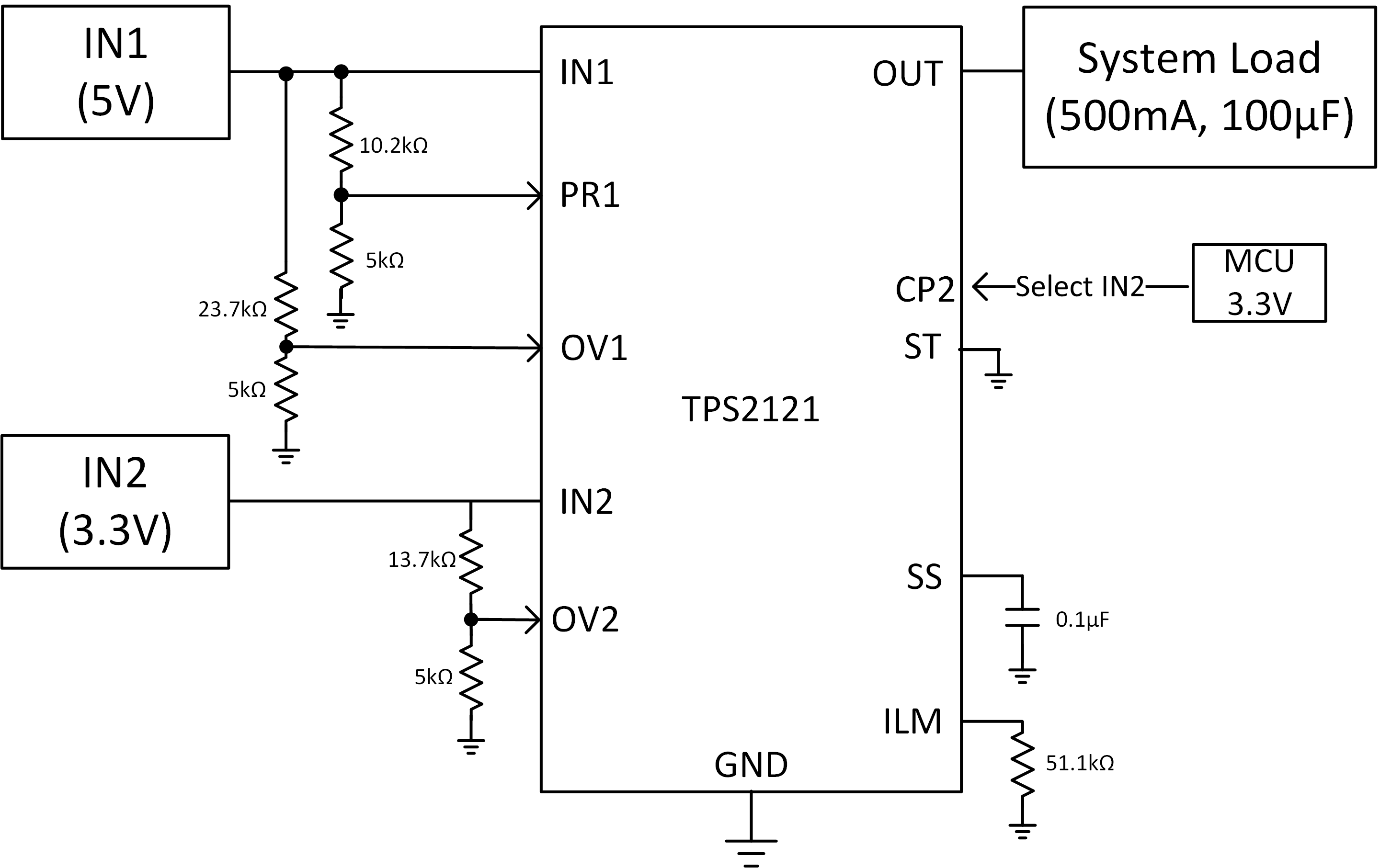
On the TPS2121, fast switchover can be enabled to minimize the voltage drop on VOUT. The internal comparator will detect and seamlessly switch between IN1 and IN2 as long as a reverse voltage condition does not exist on that channel. To enable fast switchover on the TPS2121, CP2 needs to be higher than VREF, 1.06-V (typical). By using the external voltage reference control scheme (XREF), the voltages on PR1 and CP2 pins are compared to determine whether IN1 or IN2 is powering the output. If the voltage on PR1 is higher than CP2, then IN1 is powering the output. If the voltage on PR1 is lower than CP2, then IN2 is powering the output.
Manual switchover on the TPS2121 is configured by connecting PR1 to IN1 with a resistor divider, and connecting CP2 to the external 3.3-V MCU signal. If the voltage on CP2 is higher than the voltage on PR1, then IN2 will power the output. However, if CP2 is toggled low, then IN1 will power the output, assuming IN1 has a valid input voltage.
The diagram below shows the application schematic for this design example on the TPS2121.
 Figure 10-4 TPS2121 Manual Switchover