JAJSG28F august   2018  – august 2020 TPS2120 , TPS2121

PRODUCTION DATA  

  1.   1
  2. 特長
  3. アプリケーション
  4. 概要
  5. Revision History
  6. Device Comparison Table
  7. Pin Configuration and Functions
    1.     8
  8. Specifications
    1. 7.1 Absolute Maximum Ratings
    2. 7.2 ESD Ratings
    3. 7.3 Recommended Operating Conditions
    4. 7.4 Thermal Information
    5. 7.5 Electrical Characteristics
    6. 7.6 Typical Characteristics
  9. Parameter Measurement Information
  10. Detailed Description
    1. 9.1 Overview
    2. 9.2 Functional Block Diagram
    3. 9.3 Feature Description
      1. 9.3.1 Input Settling Time and Output Soft Start Control (SS)
        1. 9.3.1.1 Slew Rate vs. CSS Capacitor
      2. 9.3.2 Active Current Limiting (ILM)
      3. 9.3.3 Short-Circuit Protection
      4. 9.3.4 Thermal Protection (TSD)
      5. 9.3.5 Overvoltage Protection (OVx)
      6. 9.3.6 Fast Reverse Current Blocking (RCB)
      7. 9.3.7 Output Voltage Dip and Fast Switchover Control (TPS2121 only)
      8. 9.3.8 Input Voltage Comparator (VCOMP)
    4. 9.4 TPS2120 Device Functional Modes
    5. 9.5 TPS2121 Device Functional Modes
  11. 10Application and Implementation
    1. 10.1 Application Information
    2. 10.2 Typical Application
      1. 10.2.1 Manual Switchover Schematic
      2. 10.2.2 Design Requirements
      3. 10.2.3 Detailed Design Description
      4. 10.2.4 Design Procedure
        1. 10.2.4.1 Selecting PR1 and CP2 Resistors
        2. 10.2.4.2 Selecting OVx Resistors
        3. 10.2.4.3 Selecting Soft-Start Capacitor and Current Limit Resistors
      5. 10.2.5 Application Curves
    3. 10.3 Automatic Switchover with Priority (XCOMP)
      1. 10.3.1 Application Schematic
      2. 10.3.2 Design Requirements
      3. 10.3.3 Detailed Design Description
      4. 10.3.4 Design Procedure
        1. 10.3.4.1 Selecting PR1 and CP2 Resistors
      5. 10.3.5 Application Curves
    4. 10.4 Automatic Seamless Switchover with Priority (XREF)
      1. 10.4.1 Application Schematic
      2. 10.4.2 Design Requirements
      3. 10.4.3 Detailed Design Description
      4. 10.4.4 Application Curves
    5. 10.5 Highest Voltage Operation (VCOMP)
      1. 10.5.1 Application Schematic
      2. 10.5.2 Design Requirements
      3. 10.5.3 Detailed Design Description
      4. 10.5.4 Detailed Design Procedure
      5. 10.5.5 Application Curves
    6. 10.6 Reverse Polarity Protection with TPS212x
    7. 10.7 Hotplugging with TPS212x
  12. 11Power Supply Recommendations
  13. 12Layout
    1. 12.1 Layout Guidelines
    2. 12.2 Layout Example
  14. 13Device and Documentation Support
    1. 13.1 Documentation Support
      1. 13.1.1 Related Links
    2. 13.2 ドキュメントの更新通知を受け取る方法
    3. 13.3 サポート・リソース
    4. 13.4 Trademarks
    5. 13.5 静電気放電に関する注意事項
    6. 13.6 用語集
  15. 14Mechanical, Packaging, and Orderable Information

パッケージ・オプション

デバイスごとのパッケージ図は、PDF版データシートをご参照ください。

メカニカル・データ(パッケージ|ピン)
  • YFP|20
サーマルパッド・メカニカル・データ
発注情報

Selecting PR1 and CP2 Resistors

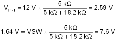
In this example, the device will switch from IN1 to IN2 when the voltage on IN1 drops below 7.6 V. Therefore, the voltage on PR1 needs to remain higher than the voltage on CP2 until this condition exists.

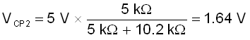
Since this example was tested on the TPS2121EVM, the resistor divider configured the voltage on CP2 to be 1.644 V.

See Equation 12 for the VCP2 Calculation

Equation 12. GUID-6E754E03-4832-4114-B4E3-0E45015DAD5C-low.gif

Since the voltage on CP2 is higher than VREF, fast switchover mode is enabled.

Next, to calculate the necessary resistor divider on PR1, the voltage on PR1 needs to drop below 1.64 V when IN1 reaches 7.6 V. On the EVM, the PR1 resistors were configured as followed:

See Equation 13 for the VPR1 Caculation

Equation 13. GUID-682802D6-777C-414C-A682-A39370E16809-low.gif