JAJSOD0A April 2022 – July 2022 TPS22811
PRODUCTION DATA
- 1 特長
- 2 アプリケーション
- 3 概要
- 4 Revision History
- 5 Pin Configuration and Functions
- 6 Specifications
-
7 Detailed Description
- 7.1 Overview
- 7.2 Functional Block Diagram
- 7.3
Feature Description
- 7.3.1 Undervoltage Lockout (UVLO and UVP)
- 7.3.2 Overvoltage Lockout (OVLO)
- 7.3.3 Inrush Current, Overcurrent, and Short-Circuit Protection
- 7.3.4 Analog Load Current Monitor
- 7.3.5 Overtemperature Protection (OTP)
- 7.3.6 Fault Response
- 7.3.7 Power-Good Indication (PG)
- 7.3.8 Quick Output Discharge (QOD)
- 7.4 Device Functional Modes
- 8 Application and Implementation
- 9 Power Supply Recommendations
- 10Layout
- 11Device and Documentation Support
- 12Mechanical, Packaging, and Orderable Information
8.2 Typical Application
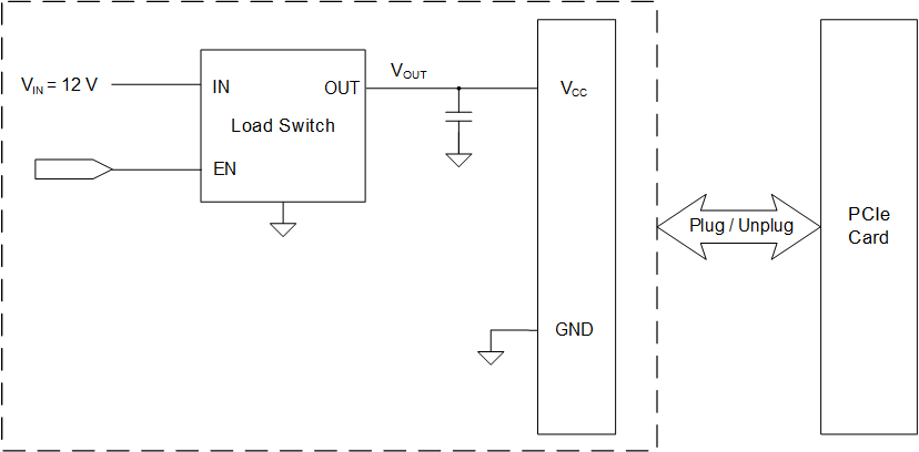
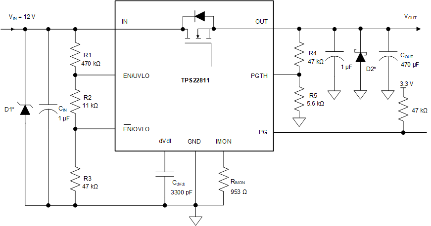
The TPS22811 device can be used in an industrial PC for input power protection of PCIe card. Industrial PCs provide flexible PCIe expansion slots with different combination of PCIe x16, PCIe x4 and PCI. PCIe x16 slot draws maximum current of up to 5.5 A from on board a 12-V rail. Load switch devices like TPS22811 can support the power requirements of these PCIe expansion slots and can be used for switching 12-V supply to PCIe card. During plugging or unplugging the PCIe card power pin of PCIe slot can short to ground that can cause the 12-V rail to droop or even damage the power tree due to very high current draw. The TPS22811 device can quickly respond to fault events like short circuit and isolate supply from load side thus preventing supply from drooping. The controlled rise time for the device greatly reduces inrush current caused by large bulk load capacitances, thereby reducing or eliminating power-supply droop.
The TPS22811 device can also be used for switching the 12-V bulk power rail of DDR5 DIMM. The PG pin of TPS22811 device can be used to enable downstream DC-DC converters after the 12-V rail is fully up.
 Figure 8-5 Power Path Protection
Block Diagram of a Typical PCIe Slot
* Optional circuit components needed for transient protection depending on input and output inductance. Please refer to Transient Protection section for details.
Figure 8-6 PCIe Expansion Slot Protection