SLVS749C November 2008 – January 2015 TPS22921 , TPS22922
UNLESS OTHERWISE NOTED, this document contains PRODUCTION DATA.
- 1 Features
- 2 Applications
- 3 Description
- 4 Typical Application
- 5 Revision History
- 6 Device Comparison Table
- 7 Pin Configuration and Functions
-
8 Specifications
- 8.1 Absolute Maximum Ratings
- 8.2 ESD Ratings
- 8.3 Recommended Operating Conditions
- 8.4 Thermal Information
- 8.5 Electrical Characteristics
- 8.6 Switching Characteristics: VIN = 0.9 V
- 8.7 Switching Characteristics: VIN = 1 V
- 8.8 Switching Characteristics: VIN = 1.1 V
- 8.9 Switching Characteristics: VIN = 1.2 V
- 8.10 Switching Characteristics: VIN = 1.8 V
- 8.11 Switching Characteristics: VIN = 2.5 V
- 8.12 Switching Characteristics: VIN = 3 V
- 8.13 Switching Characteristics: VIN = 3.6 V
- 8.14
Typical Characteristics
- 8.14.1 Typical DC Characteristics
- 8.14.2 Typical AC Characteristics (TPS22921)
- 8.14.3 Typical AC Characteristics (TPS22922)
- 8.14.4 Typical AC Characteristics (TPS22922B)
- 8.14.5 Typical AC Characteristics (TPS22921 and TPS22922)
- 8.14.6 Typical AC Characteristics (TPS22921)
- 8.14.7 Typical AC Characteristics (TPS22922)
- 8.14.8 Typical AC Characteristics (TPS22922B)
- 9 Parameter Measurement Information
- 10Detailed Description
- 11Application and Implementation
- 12Power Supply Recommendations
- 13Layout
- 14Device and Documentation Support
- 15Mechanical, Packaging, and Orderable Information
パッケージ・オプション
メカニカル・データ(パッケージ|ピン)
サーマルパッド・メカニカル・データ
発注情報
10 Detailed Description
10.1 Overview
The TPS2292x is a single-channel, 2-A load switch in a small, space-saving CSP-6 package. These devices implement a P-channel MOSFET to provide a low ON-resistance for a low voltage drop across the device. A controlled rise time is used in applications to limit the inrush current.
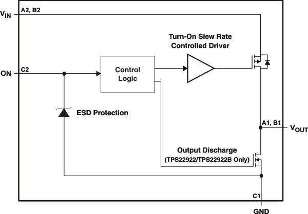
10.2 Functional Block Diagram
10.3 Feature Description
10.3.1 ON/OFF Control
The ON pin controls the state of the switch. Activating ON continuously holds the switch in the on state. ON is active high and has a low threshold making it capable of interfacing with low-voltage signals. The ON pin is compatible with standard GPIO logic threshold, and it can be used with any microcontroller with 1.2-V, 1.8-V, 2.5-V or 3.3-V GPIOs.
10.3.2 Quick Output Discharge
The TPS22922 and TPS22922B includes the Quick Output Discharge (QOD) feature. When the switch is disabled, a discharge resistance with a typical value of 65 Ω is connected between the output and ground. This resistance pulls down the output and prevents it from floating when the device is disabled.
10.4 Device Functional Modes
Table 1 lists the VOUT pin connections to for a particular device as determined by the ON pin.
Table 1. VOUT Function Table
| ON | TPS22921 | TPS22922/2B |
|---|---|---|
| L | Open | GND |
| H | VIN | VIN |