SLVS749C November 2008 – January 2015 TPS22921 , TPS22922
UNLESS OTHERWISE NOTED, this document contains PRODUCTION DATA.
- 1 Features
- 2 Applications
- 3 Description
- 4 Typical Application
- 5 Revision History
- 6 Device Comparison Table
- 7 Pin Configuration and Functions
-
8 Specifications
- 8.1 Absolute Maximum Ratings
- 8.2 ESD Ratings
- 8.3 Recommended Operating Conditions
- 8.4 Thermal Information
- 8.5 Electrical Characteristics
- 8.6 Switching Characteristics: VIN = 0.9 V
- 8.7 Switching Characteristics: VIN = 1 V
- 8.8 Switching Characteristics: VIN = 1.1 V
- 8.9 Switching Characteristics: VIN = 1.2 V
- 8.10 Switching Characteristics: VIN = 1.8 V
- 8.11 Switching Characteristics: VIN = 2.5 V
- 8.12 Switching Characteristics: VIN = 3 V
- 8.13 Switching Characteristics: VIN = 3.6 V
- 8.14
Typical Characteristics
- 8.14.1 Typical DC Characteristics
- 8.14.2 Typical AC Characteristics (TPS22921)
- 8.14.3 Typical AC Characteristics (TPS22922)
- 8.14.4 Typical AC Characteristics (TPS22922B)
- 8.14.5 Typical AC Characteristics (TPS22921 and TPS22922)
- 8.14.6 Typical AC Characteristics (TPS22921)
- 8.14.7 Typical AC Characteristics (TPS22922)
- 8.14.8 Typical AC Characteristics (TPS22922B)
- 9 Parameter Measurement Information
- 10Detailed Description
- 11Application and Implementation
- 12Power Supply Recommendations
- 13Layout
- 14Device and Documentation Support
- 15Mechanical, Packaging, and Orderable Information
パッケージ・オプション
メカニカル・データ(パッケージ|ピン)
サーマルパッド・メカニカル・データ
発注情報
8 Specifications
8.1 Absolute Maximum Ratings(1)
| MIN | MAX | UNIT | ||||
|---|---|---|---|---|---|---|
| VIN | Input voltage | –0.3 | 4 | V | ||
| VOUT | Output voltage | VIN + 0.3 | V | |||
| VON | Input voltage | –0.3 | 4 | V | ||
| P | Power dissipation at TA = 25°C | 0.645 | W | |||
| IMAX | Maximum continuous switch current | 2 | A | |||
| TA | Operating free-air temperature | –40 | 85 | °C | ||
| Tlead | Maximum lead temperature (10-s soldering time) | 300 | °C | |||
| Tstg | Storage temperature | –65 | 150 | °C | ||
(1) Stresses beyond those listed under Absolute Maximum Ratings may cause permanent damage to the device. These are stress ratings only, and functional operation of the device at these or any other conditions beyond those indicated under Recommended Operating Conditions is not implied. Exposure to absolute-maximum-rated conditions for extended periods may affect device reliability.
8.2 ESD Ratings
| VALUE | UNIT | |||
|---|---|---|---|---|
| V(ESD) | Electrostatic discharge | Human body model (HBM), per ANSI/ESDA/JEDEC JS-001(1) | ±3000 | V |
| Charged-device model (CDM), per JEDEC specification JESD22-C101(2) | ±1000 | |||
| Machine model (MM) | ±300 | |||
(1) JEDEC document JEP155 states that 500-V HBM allows safe manufacturing with a standard ESD control process.
(2) JEDEC document JEP157 states that 250-V CDM allows safe manufacturing with a standard ESD control process.
8.3 Recommended Operating Conditions
| MIN | MAX | UNIT | ||
|---|---|---|---|---|
| VIN | Input voltage range | 0.9 | 3.6 | V |
| VOUT | Output voltage range | VIN | V | |
| VIH | High-level input voltage, ON | 0.85 | 3.6 | V |
| VIL | Low-level input voltage, ON | 0.4 | V | |
| CIN | Input capacitor | 1(1) | µF |
(1) Refer to Application Information.
8.4 Thermal Information
| THERMAL METRIC(1) | TPS22921, TPS22922, TPS22922B | TPS22921 | UNIT | ||
|---|---|---|---|---|---|
| YFP | YZP | YZT | |||
| 6 PINS | |||||
| RθJA | Junction-to-ambient thermal resistance | 125.1 | 131 | 120.7 | °C/W |
| RθJC(top) | Junction-to-case (top) thermal resistance | 1.4 | 1.3 | 2.1 | |
| RθJB | Junction-to-board thermal resistance | 26 | 22.6 | 26.4 | |
| ψJT | Junction-to-top characterization parameter | 0.3 | 5.2 | 3.7 | |
| ψJB | Junction-to-board characterization parameter | 26 | 22.6 | 26.4 | |
(1) For more information about traditional and new thermal metrics, see the IC Package Thermal Metrics application report, SPRA953.
8.5 Electrical Characteristics
VIN = 0.9 V to 3.6 V, TA = –40°C to 85°C (unless otherwise noted)| PARAMETER | TEST CONDITIONS | TA | MIN | TYP(1) | MAX | UNIT | ||
|---|---|---|---|---|---|---|---|---|
| IQ | Quiescent current | IOUT = 0 mA | VIN = 1 V | Full | 30 | 120 | nA | |
| VIN = 1.8 V | Full | 78 | 235 | |||||
| VIN = 3.6 V | Full | 200 | 880 | |||||
| IIN(OFF) | OFF-state supply current | VON = GND, OUT = Open |
VIN = 1 V | Full | 10 | 210 | nA | |
| VIN = 1.8 V | Full | 35 | 260 | |||||
| VIN = 3.6 V | Full | 120 | 700 | |||||
| IIN(LEAKAGE) | OFF-state switch current | VON = GND, VOUT = 0 V |
VIN = 1 V | Full | 12 | 140 | nA | |
| VIN = 1.8 V | Full | 50 | 230 | |||||
| VIN = 3.6 V | Full | 130 | 610 | |||||
| rON | ON-state resistance | IOUT = –200 mA | VIN = 3.6 V | 25°C | 14 | 45 | mΩ | |
| Full | 50 | |||||||
| VIN = 2.5 V | 25°C | 20 | 55 | |||||
| Full | 60 | |||||||
| VIN = 1.8 V | 25°C | 33 | 65 | |||||
| Full | 75 | |||||||
| VIN = 1.2 V | 25°C | 67 | 100 | |||||
| Full | 120 | |||||||
| VIN = 1.1 V | 25°C | 82 | 150 | |||||
| Full | 160 | |||||||
| VIN = 1 V | 25°C | 116 | 160 | |||||
| Full | 170 | |||||||
| rPD | Output pulldown resistance | VIN = 3.3 V, VON = 0 V, IOUT = 30 mA (TPS22922 and TPS22922B only) |
25°C | 65 | 120 | Ω | ||
| ION | ON input leakage current | VON = 1.1 V to 3.6 V or GND | Full | 25 | nA | |||
(1) Typical values are at the specified VIN and TA = 25°C.
8.6 Switching Characteristics: VIN = 0.9 V
VIN = 0.9 V, TA = 25°C (unless otherwise noted)| PARAMETER | TEST CONDITIONS | TPS22921 | TPS22922 | TPS22922B | UNIT | ||||||||
|---|---|---|---|---|---|---|---|---|---|---|---|---|---|
| MIN | TYP | MAX | MIN | TYP | MAX | MIN | TYP | MAX | |||||
| tON | Turn-ON time | RL = 500 Ω | CL = 0.1 μF | 121 | 121 | 638 | μs | ||||||
| CL = 1 μF | 160 | 160 | 712 | ||||||||||
| CL = 3 μF | 188 | 188 | 799 | ||||||||||
| tOFF | Turn-OFF time | RL = 500 Ω | CL = 0.1 μF | 46 | 40 | 40 | μs | ||||||
| CL = 1 μF | 308 | 279 | 279 | ||||||||||
| CL = 3 μF | 975 | 807 | 807 | ||||||||||
| tr | VOUT rise time | RL = 500 Ω | CL = 0.1 μF | 60 | 60 | 462 | μs | ||||||
| CL = 1 μF | 85 | 85 | 465 | ||||||||||
| CL = 3 μF | 107 | 107 | 507 | ||||||||||
| tf | VOUT fall time | RL = 500 Ω | CL = 0.1 μF | 119 | 51 | 51 | μs | ||||||
| CL = 1 μF | 969 | 434 | 434 | ||||||||||
| CL = 3 μF | 3174 | 1264 | 1264 | ||||||||||
8.7 Switching Characteristics: VIN = 1 V
VIN = 1 V, TA = 25°C (unless otherwise noted)| PARAMETER | TEST CONDITIONS | TPS22921 | TPS22922 | TPS22922B | UNIT | ||||||||
|---|---|---|---|---|---|---|---|---|---|---|---|---|---|
| MIN | TYP | MAX | MIN | TYP | MAX | MIN | TYP | MAX | |||||
| tON | Turn-ON time | RL = 500 Ω | CL = 0.1 μF | 105 | 105 | 549 | μs | ||||||
| CL = 1 μF | 136 | 136 | 613 | ||||||||||
| CL = 3 μF | 157 | 157 | 683 | ||||||||||
| tOFF | Turn-OFF time | RL = 500 Ω | CL = 0.1 μF | 46 | 28 | 28 | μs | ||||||
| CL = 1 μF | 309 | 186 | 186 | ||||||||||
| CL = 3 μF | 983 | 511 | 511 | ||||||||||
| tr | VOUT rise time | RL = 500 Ω | CL = 0.1 μF | 51 | 51 | 386 | μs | ||||||
| CL = 1 μF | 78 | 78 | 388 | ||||||||||
| CL = 3 μF | 88 | 88 | 419 | ||||||||||
| tf | VOUT fall time | RL = 500 Ω | CL = 0.1 μF | 121 | 34 | 34 | μs | ||||||
| CL = 1 μF | 986 | 306 | 306 | ||||||||||
| CL = 3 μF | 3300 | 908 | 908 | ||||||||||
8.8 Switching Characteristics: VIN = 1.1 V
VIN = 1.1 V, TA = 25°C (unless otherwise noted)| PARAMETER | TEST CONDITIONS | TPS22921 | TPS22922 | TPS22922B | UNIT | ||||||||
|---|---|---|---|---|---|---|---|---|---|---|---|---|---|
| MIN | TYP | MAX | MIN | TYP | MAX | MIN | TYP | MAX | |||||
| tON | Turn-ON time | RL = 500 Ω | CL = 0.1 μF | 91 | 93 | 484 | μs | ||||||
| CL = 1 μF | 118 | 118 | 540 | ||||||||||
| CL = 3 μF | 137 | 137 | 599 | ||||||||||
| tOFF | Turn-OFF time | RL = 500 Ω | CL = 0.1 μF | 44 | 21 | 21 | μs | ||||||
| CL = 1 μF | 311 | 144 | 144 | ||||||||||
| CL = 3 μF | 99 | 383 | 383 | ||||||||||
| tr | VOUT rise time | RL = 500 Ω | CL = 0.1 μF | 46 | 46 | 335 | μs | ||||||
| CL = 1 μF | 60 | 60 | 336 | ||||||||||
| CL = 3 μF | 76 | 76 | 363 | ||||||||||
| tf | VOUT fall time | RL = 500 Ω | CL = 0.1 μF | 122 | 29 | 29 | μs | ||||||
| CL = 1 μF | 1000 | 224 | 224 | ||||||||||
| CL = 3 μF | 3300 | 732 | 732 | ||||||||||
8.9 Switching Characteristics: VIN = 1.2 V
VIN = 1.2 V, TA = 25°C (unless otherwise noted)| PARAMETER | TEST CONDITIONS | TPS22921 | TPS22922 | TPS22922B | UNIT | ||||||||
|---|---|---|---|---|---|---|---|---|---|---|---|---|---|
| MIN | TYP | MAX | MIN | TYP | MAX | MIN | TYP | MAX | |||||
| tON | Turn-ON time | RL = 500 Ω | CL = 0.1 μF | 83 | 83 | 435 | μs | ||||||
| CL = 1 μF | 103 | 103 | 485 | ||||||||||
| CL = 3 μF | 122 | 122 | 536 | ||||||||||
| tOFF | Turn-OFF time | RL = 500 Ω | CL = 0.1 μF | 44 | 17 | 17 | μs | ||||||
| CL = 1 μF | 312 | 117 | 117 | ||||||||||
| CL = 3 μF | 1000 | 319 | 319 | ||||||||||
| tr | VOUT rise time | RL = 500 Ω | CL = 0.1 μF | 41 | 41 | 301 | μs | ||||||
| CL = 1 μF | 54 | 54 | 302 | ||||||||||
| CL = 3 μF | 67 | 67 | 325 | ||||||||||
| tf | VOUT fall time | RL = 500 Ω | CL = 0.1 μF | 123 | 25 | 25 | μs | ||||||
| CL = 1 μF | 1000 | 214 | 214 | ||||||||||
| CL = 3 μF | 3400 | 632 | 632 | ||||||||||
8.10 Switching Characteristics: VIN = 1.8 V
VIN = 1.8 V, TA = 25°C (unless otherwise noted)| PARAMETER | TEST CONDITIONS | TPS22921 | TPS22922 | TPS22922B | UNIT | ||||||||
|---|---|---|---|---|---|---|---|---|---|---|---|---|---|
| MIN | TYP | MAX | MIN | TYP | MAX | MIN | TYP | MAX | |||||
| tON | Turn-ON time | RL = 500 Ω | CL = 0.1 μF | 54 | 54 | 282 | μs | ||||||
| CL = 1 μF | 67 | 67 | 314 | ||||||||||
| CL = 3 μF | 78 | 78 | 344 | ||||||||||
| tOFF | Turn-OFF time | RL = 500 Ω | CL = 0.1 μF | 41 | 10 | 10 | μs | ||||||
| CL = 1 μF | 312 | 67 | 67 | ||||||||||
| CL = 3 μF | 1000 | 181 | 181 | ||||||||||
| tr | VOUT rise time | RL = 500 Ω | CL = 0.1 μF | 30 | 30 | 200 | μs | ||||||
| CL = 1 μF | 37 | 37 | 202 | ||||||||||
| CL = 3 μF | 47 | 47 | 219 | ||||||||||
| tf | VOUT fall time | RL = 500 Ω | CL = 0.1 μF | 121 | 17 | 17 | μs | ||||||
| CL = 1 μF | 1000 | 158 | 158 | ||||||||||
| CL = 3 μF | 3450 | 461 | 461 | ||||||||||
8.11 Switching Characteristics: VIN = 2.5 V
VIN = 2.5 V, TA = 25°C (unless otherwise noted)| PARAMETER | TEST CONDITIONS | TPS22921 | TPS22922 | TPS22922B | UNIT | ||||||||
|---|---|---|---|---|---|---|---|---|---|---|---|---|---|
| MIN | TYP | MAX | MIN | TYP | MAX | MIN | TYP | MAX | |||||
| tON | Turn-ON time | RL = 500 Ω | CL = 0.1 μF | 40 | 40 | 211 | μs | ||||||
| CL = 1 μF | 50 | 50 | 233 | ||||||||||
| CL = 3 μF | 59 | 59 | 256 | ||||||||||
| tOFF | Turn-OFF time | RL = 500 Ω | CL = 0.1 μF | 41 | 10 | 10 | μs | ||||||
| CL = 1 μF | 316 | 56 | 56 | ||||||||||
| CL = 3 μF | 1000 | 153 | 153 | ||||||||||
| tr | VOUT rise time | RL = 500 Ω | CL = 0.1 μF | 23 | 23 | 164 | μs | ||||||
| CL = 1 μF | 29 | 29 | 165 | ||||||||||
| CL = 3 μF | 38 | 38 | 177 | ||||||||||
| tf | VOUT fall time | RL = 500 Ω | CL = 0.1 μF | 122 | 16 | 16 | μs | ||||||
| CL = 1 μF | 1086 | 147 | 147 | ||||||||||
| CL = 3 μF | 3600 | 430 | 430 | ||||||||||
8.12 Switching Characteristics: VIN = 3 V
VIN = 3 V, TA = 25°C (unless otherwise noted)| PARAMETER | TEST CONDITIONS | TPS22921 | TPS22922 | TPS22922B | UNIT | ||||||||
|---|---|---|---|---|---|---|---|---|---|---|---|---|---|
| MIN | TYP | MAX | MIN | TYP | MAX | MIN | TYP | MAX | |||||
| tON | Turn-ON time | RL = 500 Ω | CL = 0.1 μF | 30 | 30 | 182 | μs | ||||||
| CL = 1 μF | 38 | 38 | 201 | ||||||||||
| CL = 3 μF | 45 | 45 | 221 | ||||||||||
| tOFF | Turn-OFF time | RL = 500 Ω | CL = 0.1 μF | 40 | 10 | 10 | μs | ||||||
| CL = 1 μF | 353 | 51 | 51 | ||||||||||
| CL = 3 μF | 1036 | 139 | 139 | ||||||||||
| tr | VOUT rise time | RL = 500 Ω | CL = 0.1 μF | 20 | 20 | 149 | μs | ||||||
| CL = 1 μF | 25 | 25 | 150 | ||||||||||
| CL = 3 μF | 33 | 33 | 161 | ||||||||||
| tf | VOUT fall time | RL = 500 Ω | CL = 0.1 μF | 104 | 15 | 15 | μs | ||||||
| CL = 1 μF | 1030 | 143 | 143 | ||||||||||
| CL = 3 μF | 3230 | 419 | 419 | ||||||||||
8.13 Switching Characteristics: VIN = 3.6 V
VIN = 3.6 V, TA = 25°C (unless otherwise noted)| PARAMETER | TEST CONDITIONS | TPS22921 | TPS22922 | TPS22922B | UNIT | ||||||||
|---|---|---|---|---|---|---|---|---|---|---|---|---|---|
| MIN | TYP | MAX | MIN | TYP | MAX | MIN | TYP | MAX | |||||
| tON | Turn-ON time | RL = 500 Ω | CL = 0.1 μF | 30 | 30 | 159 | μs | ||||||
| CL = 1 μF | 38 | 38 | 175 | ||||||||||
| CL = 3 μF | 45 | 45 | 193 | ||||||||||
| tOFF | Turn-OFF time | RL = 500 Ω | CL = 0.1 μF | 42 | 10 | 10 | μs | ||||||
| CL = 1 μF | 310 | 51 | 51 | ||||||||||
| CL = 3 μF | 988 | 139 | 139 | ||||||||||
| tr | VOUT rise time | RL = 500 Ω | CL = 0.1 μF | 20 | 20 | 137 | μs | ||||||
| CL = 1 μF | 25 | 25 | 138 | ||||||||||
| CL = 3 μF | 33 | 33 | 148 | ||||||||||
| tf | VOUT fall time | RL = 500 Ω | CL = 0.1 μF | 120 | 15 | 15 | μs | ||||||
| CL = 1 μF | 1100 | 143 | 143 | ||||||||||
| CL = 3 μF | 3600 | 419 | 419 | ||||||||||
8.14 Typical Characteristics
8.14.1 Typical DC Characteristics
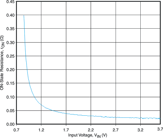 Figure 1. rON vs VIN
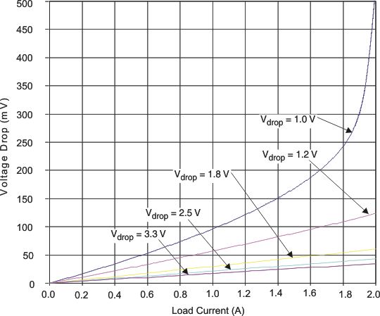 Figure 3. Voltage Drop vs Load Current
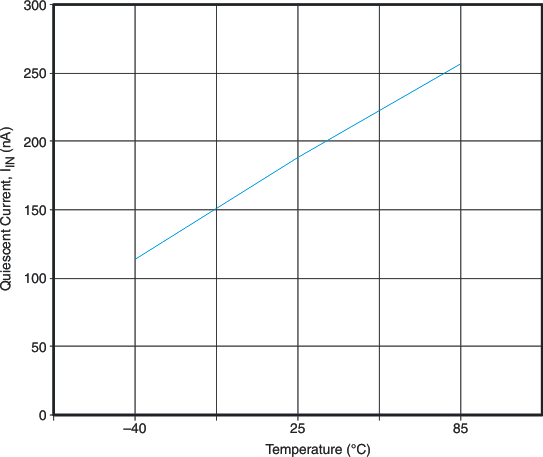 Figure 5. Quiescent Current vs Temperature
(VIN = 3.3 V, IOUT = 0 mA)
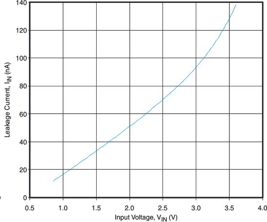 Figure 7. Leakage Current vs VIN
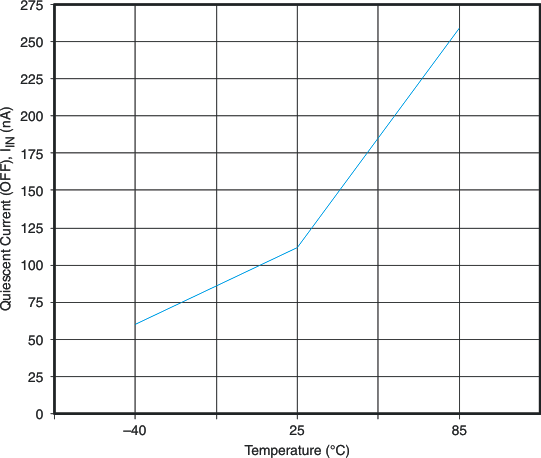 Figure 9. IIN (OFF) vs Temperature (VIN = 3.3 V)
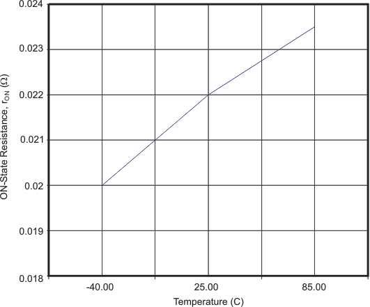 Figure 2. rON vs Temperature (VIN = 3.3 V)
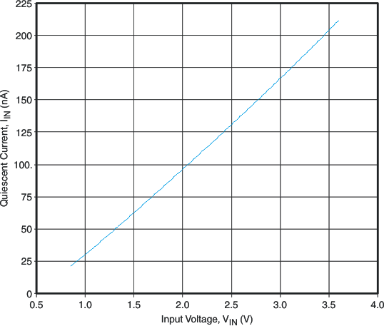 Figure 4. Quiescent Current vs VIN (VON = VIN)
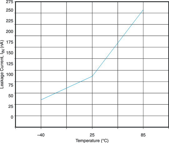 Figure 6. IIN Leakage Current vs Temperature (VIN = 3.3 V)
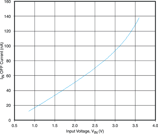 Figure 8. IIN (OFF) vs VIN (VON = 0 V)
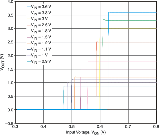 Figure 10. ON-Input Threshold
8.14.2 Typical AC Characteristics (TPS22921)
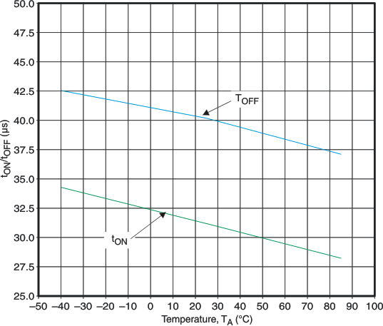 Figure 11. tON/tOFF vs Temperature (VIN = 3.3 V)
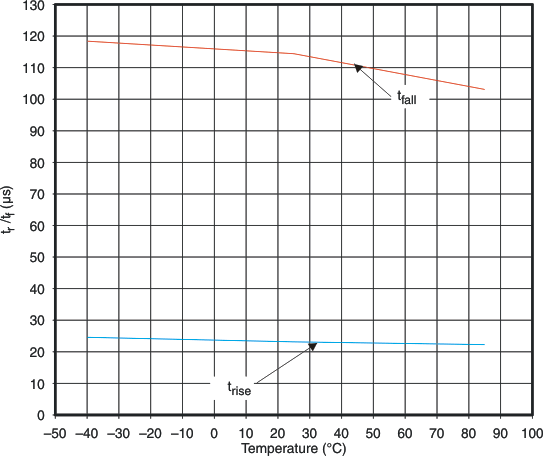 Figure 12. trise/tfall vs Temperature (VIN = 3.3 V)
8.14.3 Typical AC Characteristics (TPS22922)
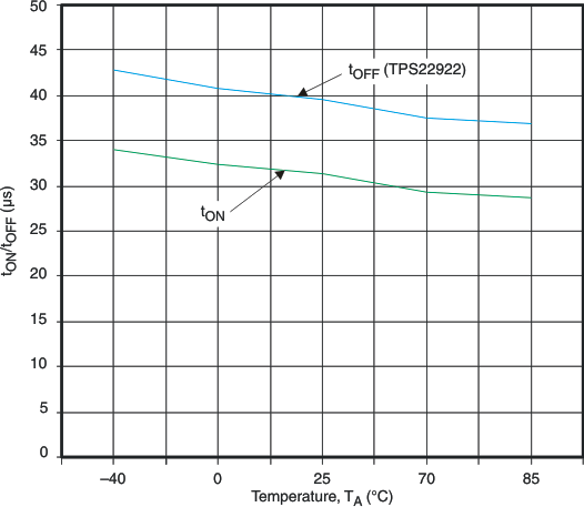 Figure 13. tON/tOFF vs Temperature (VIN = 3.3 V)
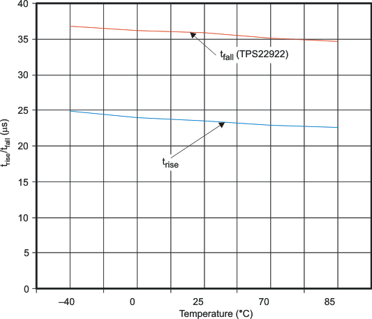 Figure 14. trise/tfall vs Temperature (VIN = 3.3 V)
8.14.4 Typical AC Characteristics (TPS22922B)
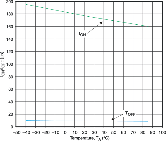 Figure 15. tON/tOFF vs Temperature (VIN = 3.3 V)
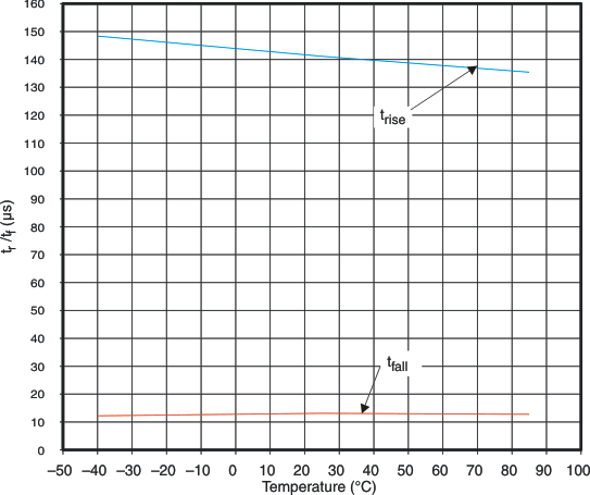 Figure 16. trise/tfall vs Temperature (VIN = 3.3 V)
8.14.5 Typical AC Characteristics (TPS22921 and TPS22922)
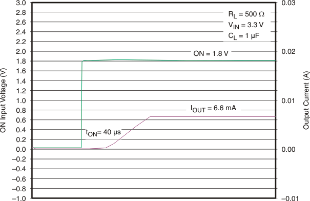 Figure 17. tON Response
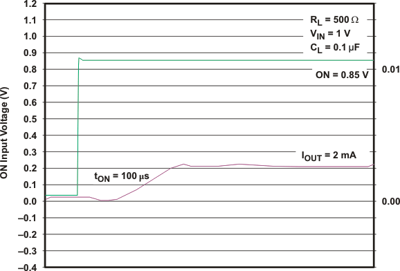 Figure 19. tON Response
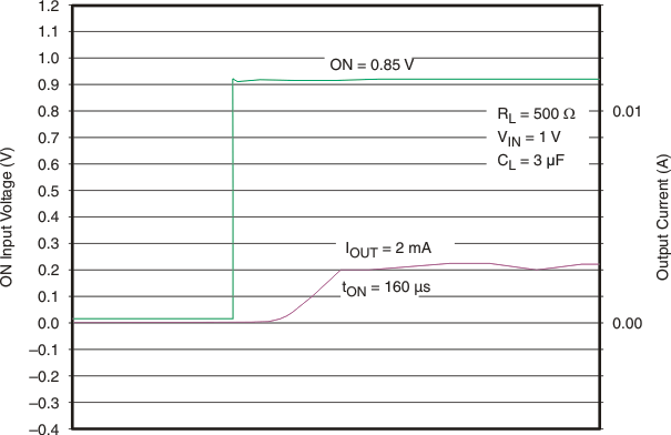 Figure 21. tON Response
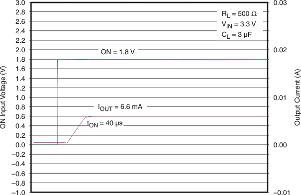 Figure 18. tON Response
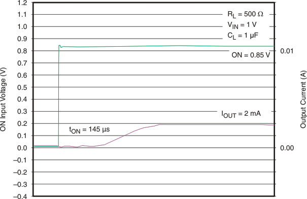 Figure 20. tON Response
8.14.6 Typical AC Characteristics (TPS22921)
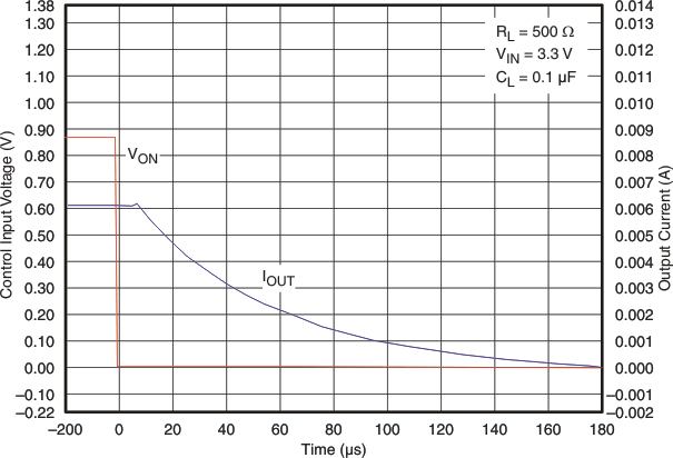 Figure 22. tOFF Response
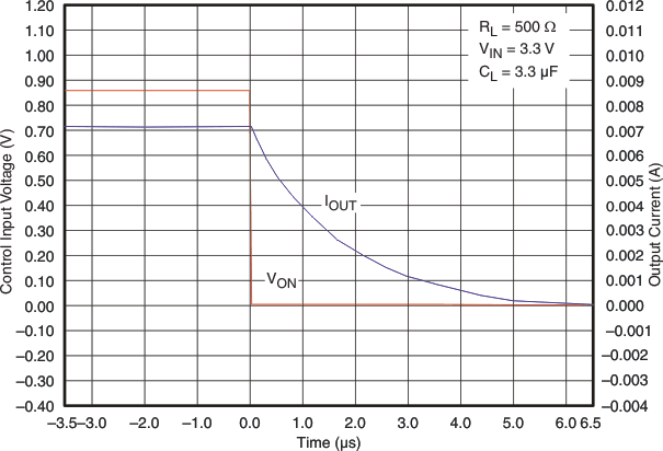 Figure 24. tOFF Response
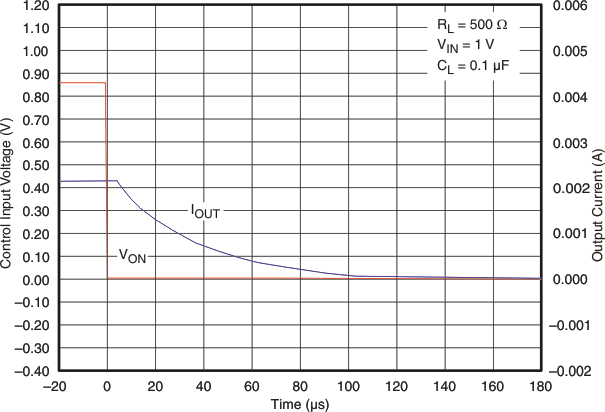 Figure 26. tOFF Response
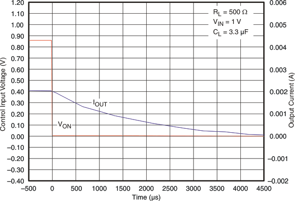 Figure 28. tOFF Response
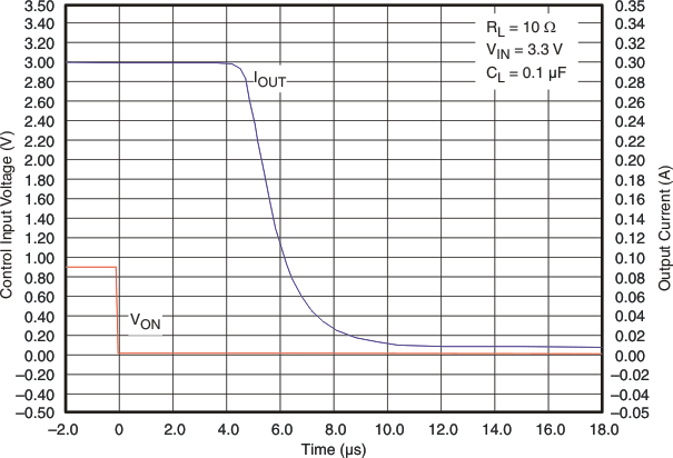 Figure 23. tOFF Response
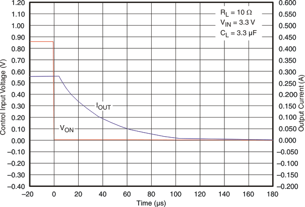 Figure 25. tOFF Response
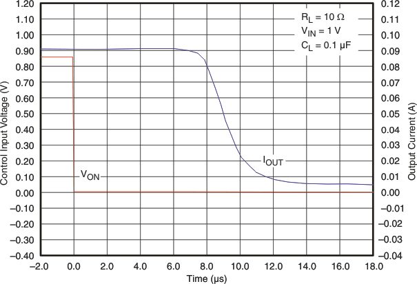 Figure 27. tOFF Response
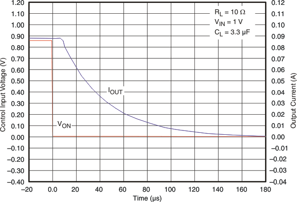 Figure 29. tOFF Response
8.14.7 Typical AC Characteristics (TPS22922)
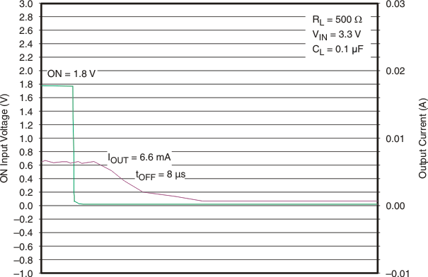 Figure 30. tOFF Response
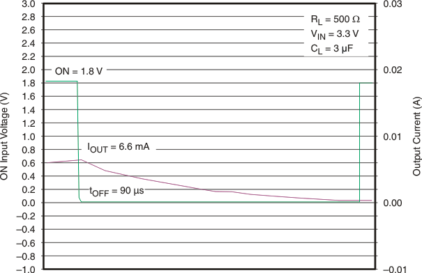 Figure 32. tOFF Response
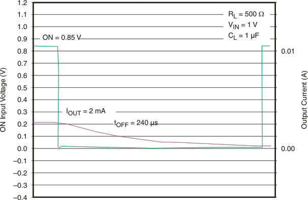 Figure 34. tOFF Response
 Figure 31. tOFF Response
 Figure 33. tOFF Response
 Figure 35. tOFF Response
8.14.8 Typical AC Characteristics (TPS22922B)
 Figure 36. tON Response
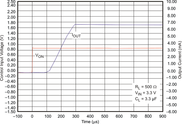 Figure 38. tON Response
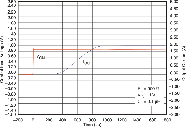 Figure 40. tON Response
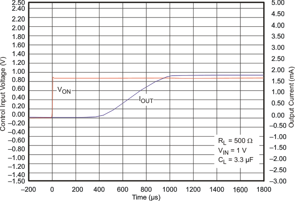 Figure 42. tON Response
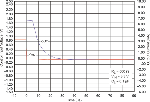 Figure 44. tOFF Response
 Figure 46. tOFF Response
 Figure 48. tOFF Response
 Figure 37. tON Response
 Figure 39. tON Response
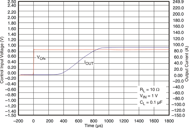 Figure 41. tON Response
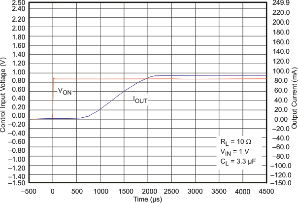 Figure 43. tON Response
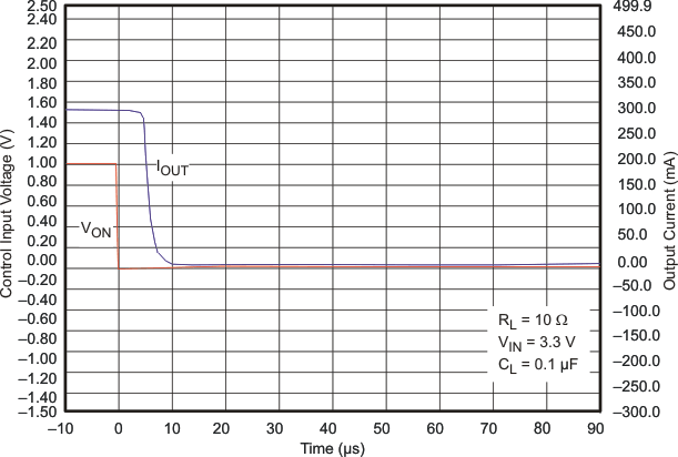 Figure 45. tOFF Response
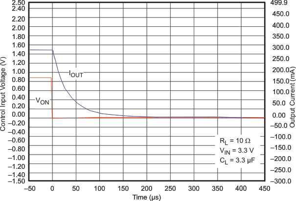 Figure 47. tOFF Response
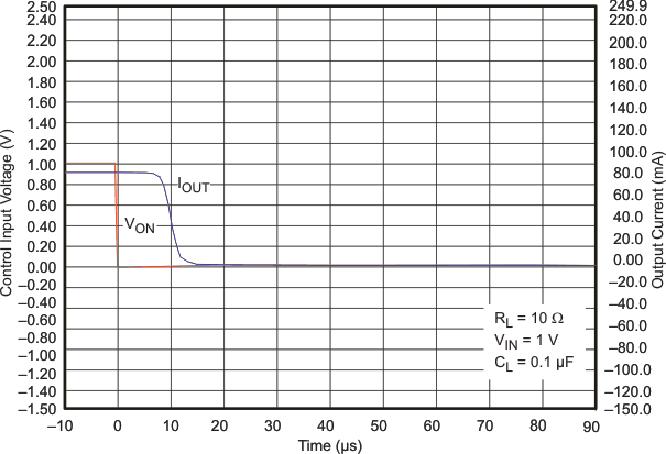 Figure 49. tOFF Response
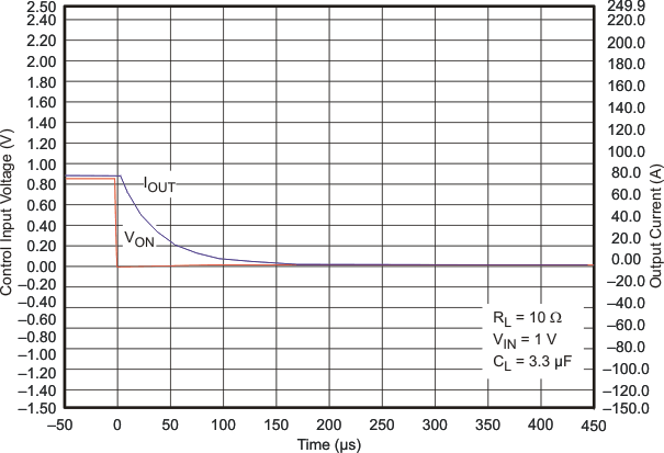 Figure 51. tOFF Response