SLVSCT5D March 2015 – September 2016 TPS22953 , TPS22954
PRODUCTION DATA.
- 1 Features
- 2 Applications
- 3 Description
- 4 Revision History
- 5 Device Comparison Table
- 6 Pin Configuration and Functions
-
7 Specifications
- 7.1 Absolute Maximum Ratings
- 7.2 ESD Ratings
- 7.3 Recommended Operating Conditions
- 7.4 Thermal Information
- 7.5 Electrical Characteristics
- 7.6 Electrical Characteristics—VBIAS = 5 V
- 7.7 Electrical Characteristics—VBIAS = 3.3 V
- 7.8 Electrical Characteristics—VBIAS = 2.5 V
- 7.9 Switching Characteristics—CT = 1000 pF
- 7.10 Switching Characteristics—CT = 0 pF
- 7.11 Typical DC Characteristics
- 7.12 Typical Switching Characteristics
- 8 Parameter Measurement Information
-
9 Detailed Description
- 9.1 Overview
- 9.2 Functional Block Diagram
- 9.3
Feature Description
- 9.3.1 On and Off Control (EN pin)
- 9.3.2 Voltage Monitoring (SNS Pin)
- 9.3.3 Power Good (PG Pin)
- 9.3.4 Supervisor Fault Detection and Automatic Restart
- 9.3.5 Manual Restart
- 9.3.6 Thermal Shutdown
- 9.3.7 Reverse Current Blocking (TPS22953 Only)
- 9.3.8 Quick Output Discharge (QOD) (TPS22954 Only)
- 9.3.9 VIN and VBIAS Voltage Range
- 9.3.10 Adjustable Rise Time (CT pin)
- 9.3.11 Power Sequencing
- 9.4 Device Functional Modes
- 10Application and Implementation
- 11Power Supply Recommendations
- 12Layout
- 13Device and Documentation Support
- 14Mechanical, Packaging, and Orderable Information
パッケージ・オプション
メカニカル・データ(パッケージ|ピン)
サーマルパッド・メカニカル・データ
- DQC|10
発注情報
12 Layout
12.1 Layout Guidelines
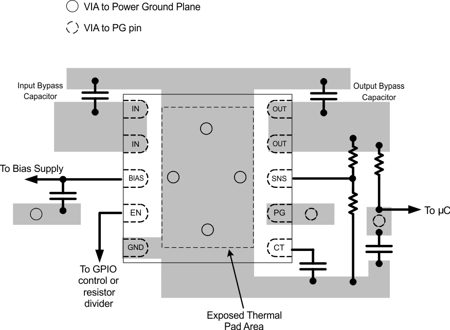
- Input and Output traces must be as short and wide as possible to accommodate for high current.
- Use vias under the exposed thermal pad for thermal relief for high current operation.
- The CT Capacitor must be placed as close as possible to the device to minimize parasitic trace capacitance. It is also recommended to cutout copper on other layers directly below CT to minimize parasitic capacitance.
- The IN terminal must be bypassed to ground with low ESR ceramic bypass capacitors. The typical recommended bypass capacitance is ceramic with X5R or X7R dielectric. This capacitor must be placed as close to the device pins as possible.
- The OUT terminal must be bypassed to ground with low ESR ceramic bypass capacitors. The typical recommended bypass capacitance is ceramic with X5R or X7R dielectric. This capacitor must be placed as close to the device pins as possible.
- The BIAS terminal must be bypassed to ground with low ESR ceramic bypass capacitors. The typical recommended bypass capacitance is ceramic with X5R or X7R dielectric.
12.2 Layout Example
 Figure 71. Recommended Board Layout