JAJSE14B October 2017 – November 2017 TPS23525
PRODUCTION DATA.
- 1 特長
- 2 アプリケーション
- 3 概要
- 4 改訂履歴
- 5 Pin Configuration and Functions
- 6 Specifications
- 7 Parameter Measurement Information
- 8 Detailed Description
-
9 Application and Implementation
- 9.1 Application Information
- 9.2
Typical Application
- 9.2.1 Design Requirements
- 9.2.2
Detailed Design Procedure
- 9.2.2.1 Selecting RSNS
- 9.2.2.2 Selecting Soft Start Setting: CSS and CSS,VEE
- 9.2.2.3 Selecting VDS Switch Over Threshold
- 9.2.2.4 Timer Selection
- 9.2.2.5 MOSFET Selection and SOA Checks
- 9.2.2.6 Input Cap, Input TVS, and OR-ing FET selection
- 9.2.2.7 EMI Filter Consideration
- 9.2.2.8 Under Voltage and Over Voltage Settings
- 9.2.2.9 Choosing RVCC and CVCC
- 9.2.2.10 Power Good Interface to Downstream DC/DC
- 9.2.3 Application Curves
- 10Power Supply Recommendations
- 11Layout
- 12デバイスおよびドキュメントのサポート
- 13メカニカル、パッケージ、および注文情報
8.3.2 Soft Start Disconnect
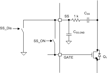
The inrush current into the output capacitor (COUT) can be limited by placing a capacitor between the SS (Soft Start) pin and the drain of the hot swap MOSFET. In that case the inrush current can be computed using equation below.

Note that with most hot swap the CSS pin is tied simply to the gate pin, but this can interfere with performance during normal operation if transients or short circuits are encountered. In addition the CSS capacitor tends to pull up the gate during hot plug and cause shoot through current if it is always tied to the gate. For that reason the TPS23525 has a disconnect switch between the gate pin and the SS pin as well as a discharge resistor. During the initial hot plug and during the insertion delay the switch between SS and GATE is open and SS is being discharged to GND through a resistor. Then during start-up SS and GATE are connected to limit the slew rate. Once in normal operation the SS pin is not tied to GATE and it is not shorted to GND, which prevents it from interfering with the operation during transients.
 Figure 9. Implementation of SS Disconnect