JAJSJE8A May   2021  – March 2022 TPS25830A-Q1 , TPS25832A-Q1

PRODUCTION DATA  

  1. 特長
  2. アプリケーション
  3. 概要
  4. Revision History
  5. 概要 (続き)
  6. Device Comparison Table
  7. Pin Configuration and Functions
  8. Specifications
    1. 8.1 Absolute Maximum Ratings
    2. 8.2 ESD Ratings
    3. 8.3 Recommended Operating Conditions
    4. 8.4 Thermal Information
    5. 8.5 Electrical Characteristics
    6. 8.6 Timing Requirements
    7. 8.7 Switching Characteristics
    8. 8.8 Typical Characteristics
  9. Parameter Measurement Information
  10. 10Detailed Description
    1. 10.1 Overview
    2. 10.2 Functional Block Diagram
    3. 10.3 Feature Description
      1. 10.3.1  Buck Regulator
      2. 10.3.2  Enable/UVLO and Start-Up
      3. 10.3.3  Switching Frequency and Synchronization (RT/SYNC)
      4. 10.3.4  Spread-Spectrum Operation
      5. 10.3.5  VCC, VCC_UVLO
      6. 10.3.6  Minimum ON-Time, Minimum OFF-Time
      7. 10.3.7  Internal Compensation
      8. 10.3.8  Bootstrap Voltage (BOOT)
      9. 10.3.9  RSNS, RSET, RILIMIT and RIMON
      10. 10.3.10 Overcurrent and Short Circuit Protection
        1. 10.3.10.1 Current Limit Setting using RILIMIT
        2. 10.3.10.2 Current Limit Setting for MFI OCP
        3. 10.3.10.3 Buck Average Current Limit Design Example
        4. 10.3.10.4 External MOSFET Gate Drivers
        5. 10.3.10.5 Cycle-by-Cycle Buck Current Limit
      11. 10.3.11 Overvoltage, IEC and Short to Battery Protection
        1. 10.3.11.1 VBUS and VCSN/OUT Overvoltage Protection
        2. 10.3.11.2 DP_IN and DM_IN Protection
        3. 10.3.11.3 CC IEC and OVP Protection
      12. 10.3.12 Cable Compensation
        1. 10.3.12.1 Cable Compensation Design Example
      13. 10.3.13 USB Port Control
      14. 10.3.14 FAULT Response
      15. 10.3.15 USB Specification Overview
      16. 10.3.16 USB Type-C® Basics
        1. 10.3.16.1 Configuration Channel
        2. 10.3.16.2 Detecting a Connection
        3. 10.3.16.3 Configuration Channel Pins CC1 and CC2
        4. 10.3.16.4 Current Capability Advertisement and VCONN Overload Protection
        5. 10.3.16.5 Plug Polarity Detection
      17. 10.3.17 Device Power Pins (IN, CSN/OUT, and PGND)
      18. 10.3.18 Thermal Shutdown
      19. 10.3.19 Power Wake
    4. 10.4 Device Functional Modes
      1. 10.4.1 Shutdown Mode
      2. 10.4.2 Standby Mode
      3. 10.4.3 Active Mode
      4. 10.4.4 Device Truth Table (TT)
      5. 10.4.5 USB Port Operating Modes
        1. 10.4.5.1 USB Type-C® Mode
        2. 10.4.5.2 Standard Downstream Port (SDP) Mode — USB 2.0, USB 3.0, and USB 3.1
        3. 10.4.5.3 Charging Downstream Port (CDP) Mode
        4. 10.4.5.4 Client Mode
      6. 10.4.6 High-Bandwidth Data-Line Switches
  11. 11Application and Implementation
    1. 11.1 Application Information
    2. 11.2 Typical Application
      1. 11.2.1 Design Requirements
      2. 11.2.2 Detailed Design Procedure
        1. 11.2.2.1  Output Voltage
        2. 11.2.2.2  Switching Frequency
        3. 11.2.2.3  Inductor Selection
        4. 11.2.2.4  Output Capacitor Selection
        5. 11.2.2.5  Input Capacitor Selection
        6. 11.2.2.6  Bootstrap Capacitor Selection
        7. 11.2.2.7  VCC Capacitor Selection
        8. 11.2.2.8  Enable and Undervoltage Lockout Set-Point
        9. 11.2.2.9  Current Limit Set-Point
        10. 11.2.2.10 Cable Compensation Set-Point
        11. 11.2.2.11 LD_DET, POL, and FAULT Resistor Selection
      3. 11.2.3 Application Curves
  12. 12Power Supply Recommendations
  13. 13Layout
    1. 13.1 Layout Guidelines
    2. 13.2 Ground Plane and Thermal Considerations
    3. 13.3 Layout Example
  14. 14Device and Documentation Support
    1. 14.1 Documentation Support
      1. 14.1.1 Related Documentation
    2. 14.2 Related Links
    3. 14.3 ドキュメントの更新通知を受け取る方法
    4. 14.4 サポート・リソース
    5. 14.5 Trademarks
    6. 14.6 静電気放電に関する注意事項
    7. 14.7 用語集
  15. 15Mechanical, Packaging, and Orderable Information

パッケージ・オプション

メカニカル・データ(パッケージ|ピン)
サーマルパッド・メカニカル・データ
発注情報

Application Curves

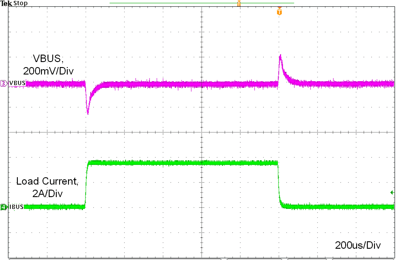
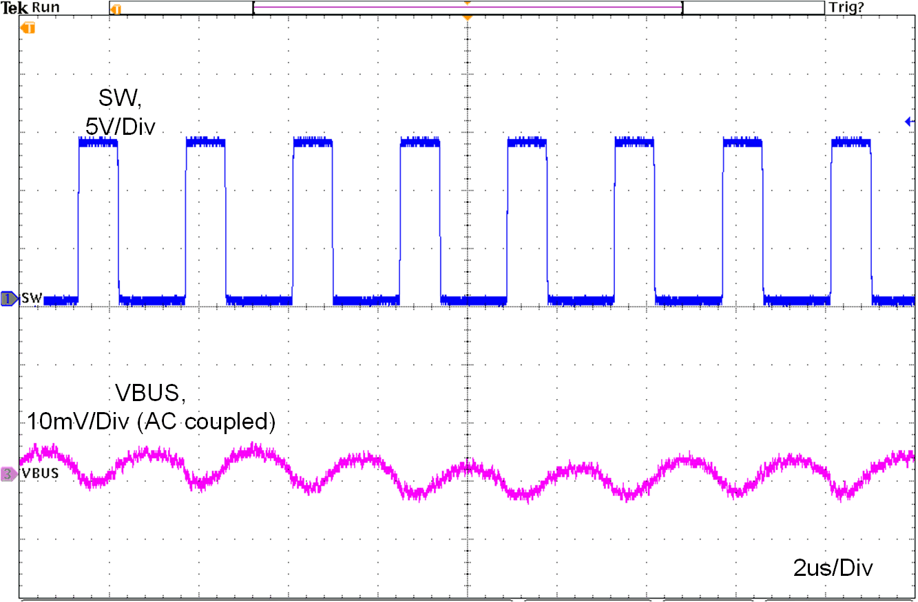
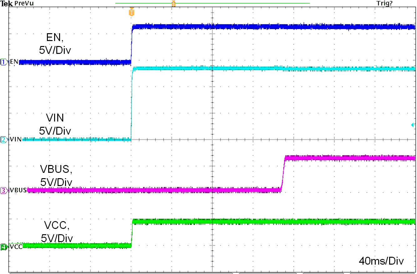
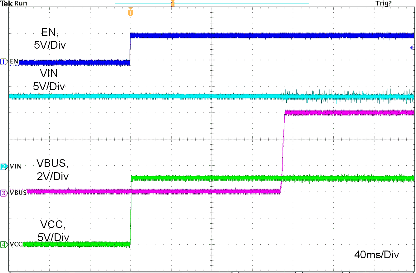
Unless otherwise specified the following conditions apply: VIN = 13.5 V, fSW = 400 kHz, L = 8.2 µH, COUT_CSP = 66 µF, COUT_CSN = 0.1 µF, CBUS = 1 µF, TA = 25 °C.
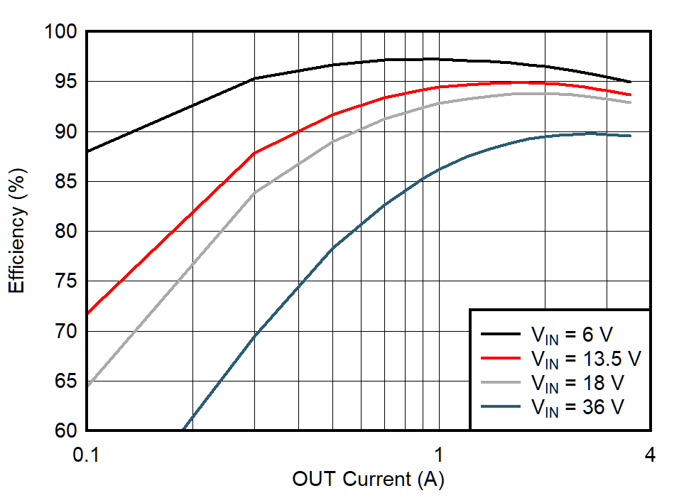
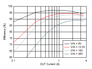
Unless otherwise specified the following conditions apply: VIN = 13.5 V, fSW = 400 kHz, L = 8.2 µH, COUT_CSP = 66 µF, COUT_CSN = 0.1 µF, CBUS = 1 µF, TA = 25 °C.GUID-F224EC24-0977-4DDD-8C74-3A60CA8D8EE7-low.png
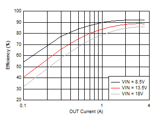
VOUT = 5.1 V fSW = 400 kHz
Figure 11-2 Buck Only Efficiency. Unless otherwise specified the following conditions apply: VIN = 13.5 V, fSW = 400 kHz, L = 8.2 µH, COUT_CSP = 66 µF, COUT_CSN = 0.1 µF, CBUS = 1 µF, TA = 25 °C.
GUID-173285AD-8DA0-48C2-A524-B352BE8EAA2E-low.gif
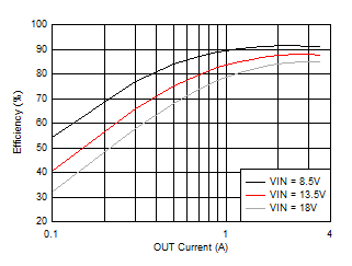
RSENS = 15 mΩ fSW = 400 kHz
Figure 11-4 Efficiency With Sense Resistor
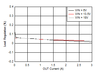
GUID-426C3304-7466-47F2-947D-BDAFA9240242-low.gif
VOUT = 5.1 V fSW = 400 kHz
Figure 11-6 Load Regulation
GUID-A65C4BBB-C86E-44F3-9F09-ACAD2775B16A-low.gif
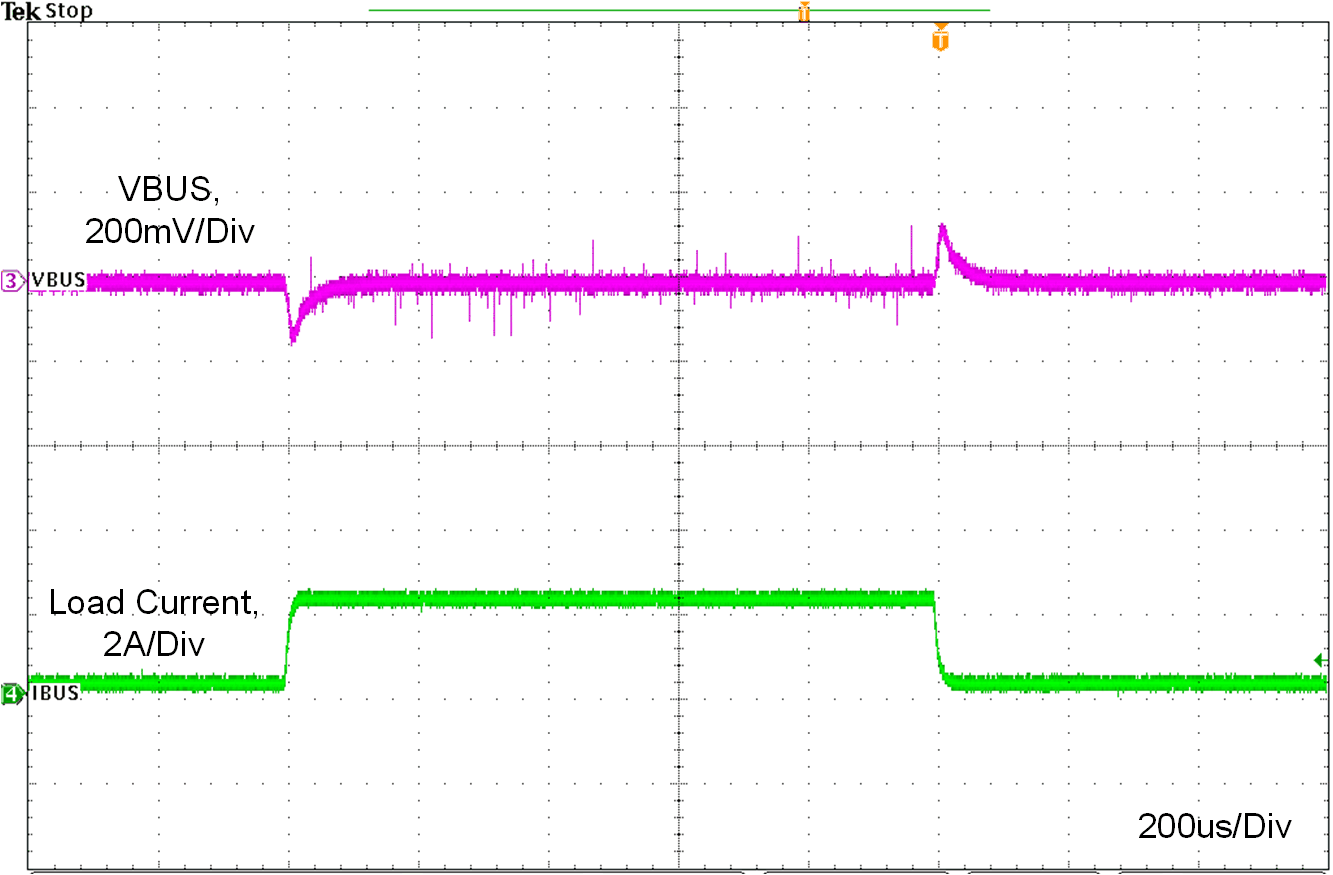
ILOAD = 0 A to 3.5 A RIMON = 0 Ω
Figure 11-8 Load Transient Without Cable Compensation
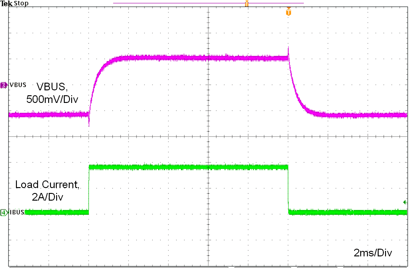
GUID-DF2D89BB-2C69-4B20-8548-F67E012F0B54-low.gif
ILOAD = 0 A to 3.5 A RIMON = 13 kΩ
Figure 11-10 Load Transient with Cable Compensation
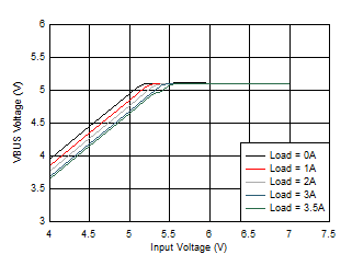
GUID-98D10D3B-5C0A-46F0-A1C4-6EF0B6E745B8-low.gif
Figure 11-12 Dropout Characteristic
GUID-B10AD6D4-8907-4878-8A2A-FD7EBF475E22-low.gif
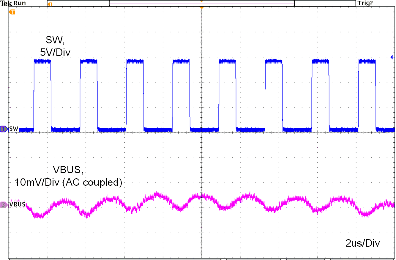
RIMON = 13 kΩ
Figure 11-14 100-mA Output Ripple
GUID-E1B77D87-43A7-41BB-B620-4382CECE00F4-low.gif
VIN = 0 V to 13.5 V CC1 = Rd ILOAD = 3 A
Figure 11-16 Startup Relate to VIN
GUID-A0C6ACCC-15D6-4DA2-B185-1FD2D37461B4-low.gif
EN = 0 V to 5 V CC1 = Rd ILOAD = 3 A
Figure 11-18 Startup Relate to EN
GUID-57E7D170-31FD-4AE4-A4C4-C4368221BBA5-low.gif
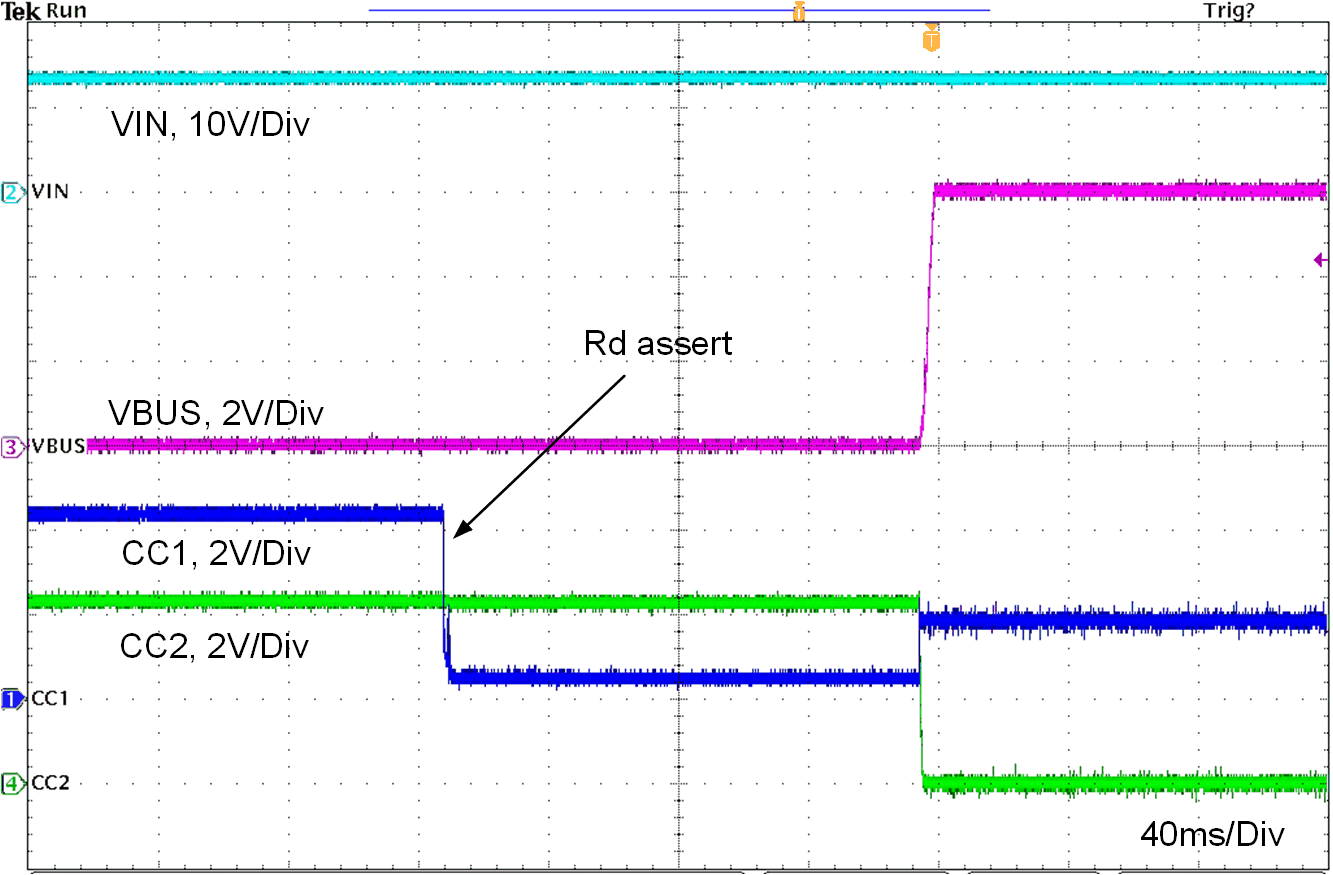
CC1 = Open to Rd CC2 = Open ILOAD = 3 A
Figure 11-20 Rd Assert
GUID-20210504-CA0I-2MJQ-XR8V-N82HSD07T5M5-low.gif
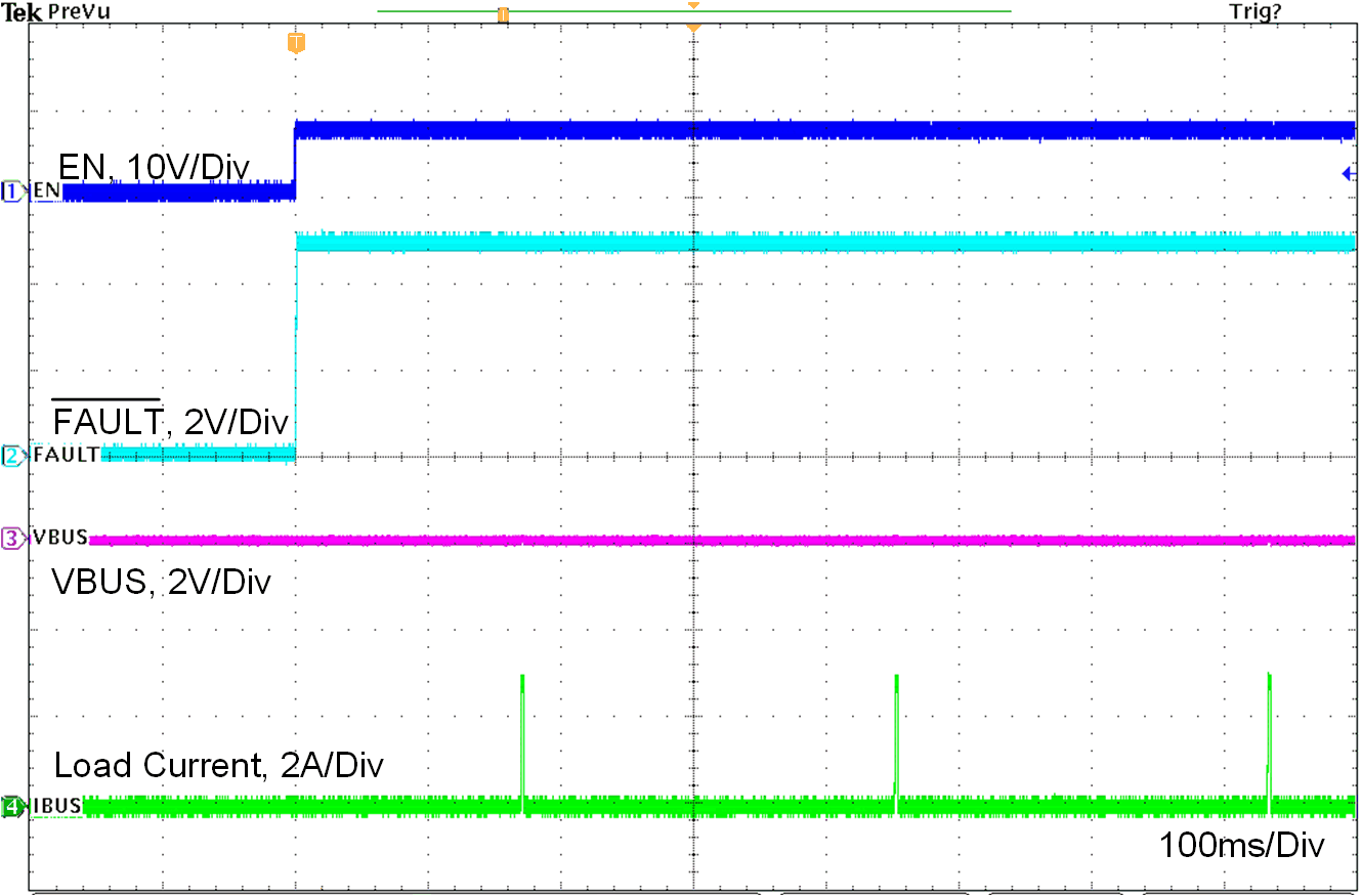
EN to High VBUS = GND RLIMIT = 13 kΩ
Figure 11-22 Enable Into Short Without External FET
GUID-20210504-CA0I-4T9C-QTCL-QVSNQHXSKH7W-low.gif
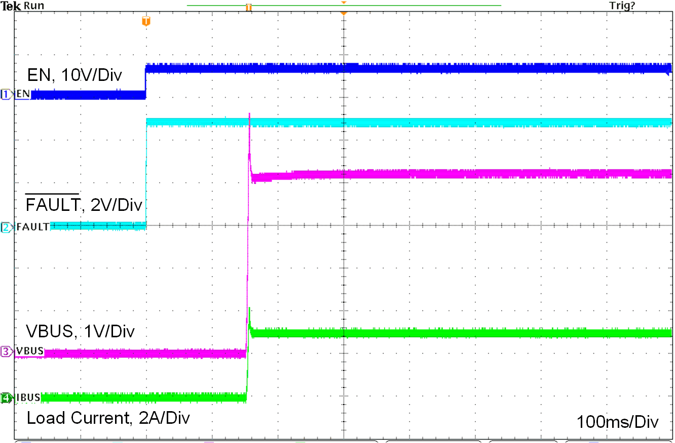
EN to High VBUS = GND RLIMIT = 13 kΩ
Figure 11-24 Enable Into 1-Ω Load Without External FET
GUID-20210504-CA0I-FF3B-WFRL-LB73HMCPNRFM-low.gif
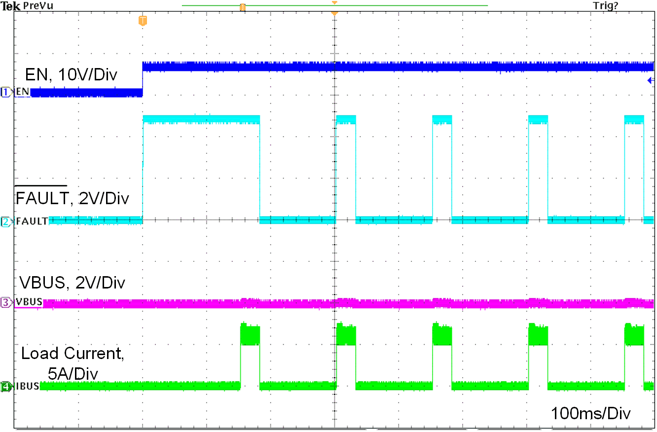
EN to High VBUS = GND RLIMIT = 6.8 kΩ
Figure 11-26 Enable Into Short With External FET
GUID-20210504-CA0I-MWVT-DKGM-ZXTZXXKBKCV1-low.gif
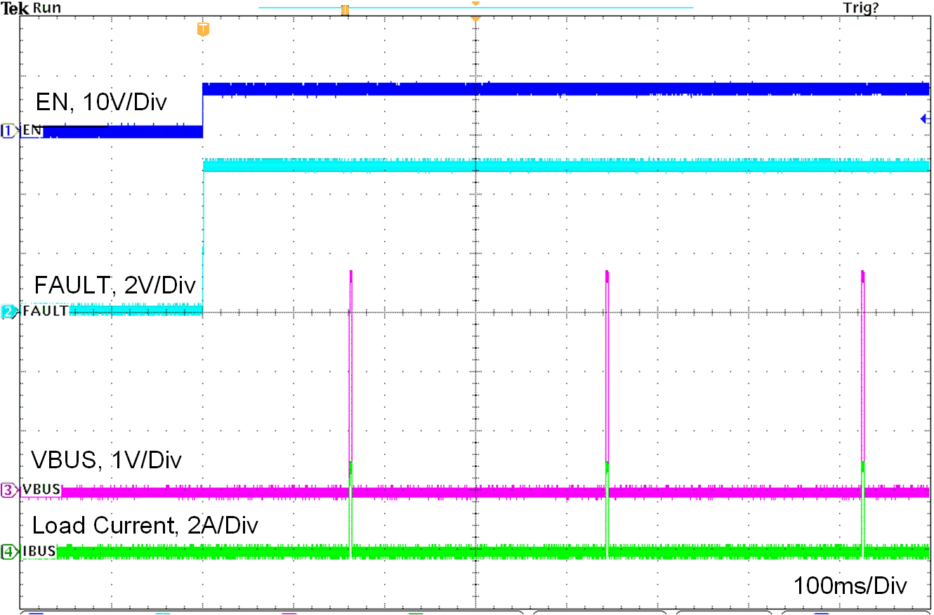
EN to High VBUS = GND RLIMIT = 6.8 kΩ
Figure 11-28 Enable Into 1-Ω Load With External FET
GUID-20210504-CA0I-Q9ZJ-PWZT-T6RXXPK4G9FJ-low.gif
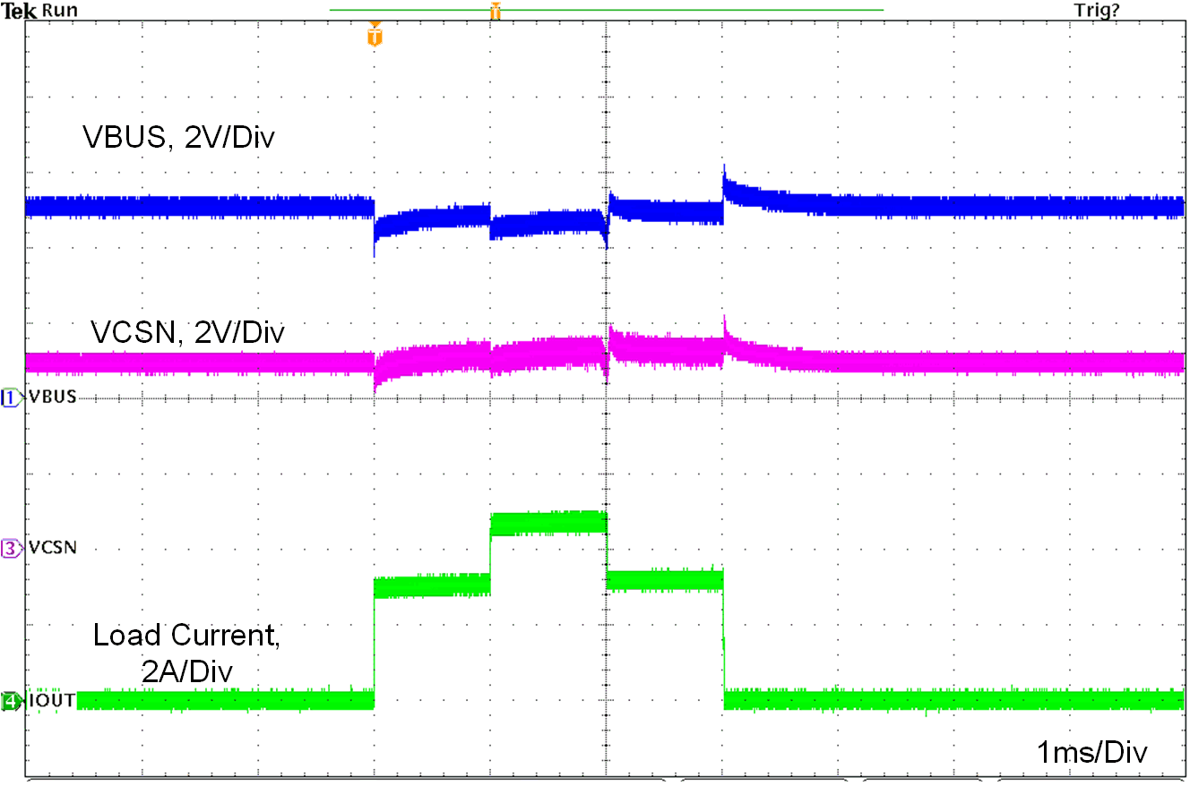
ILOAD1 = 3 A ILOAD2 = 4.8 A RLIMIT = 13 kΩ
Figure 11-30 MFI Over-Current Test Without External FET
GUID-20210504-CA0I-F7PD-ZLTK-DRRQZK6B9BKS-low.gif
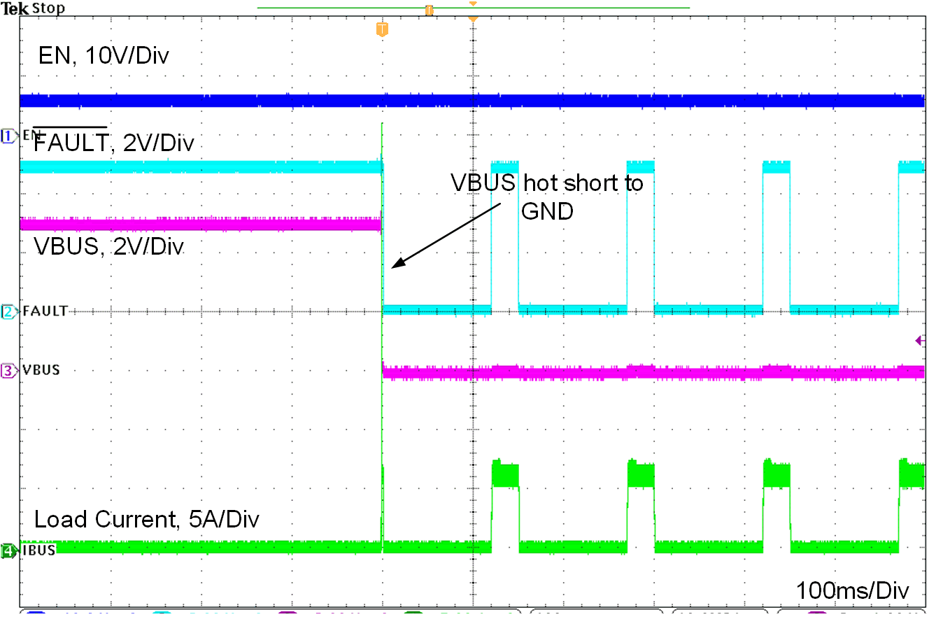
RLIMIT = 13 kΩ
Figure 11-32 VBUS Hot Short to GND Without External FET
GUID-3C46BB68-7586-4EC3-8F1B-D12DCC88705D-low.gif
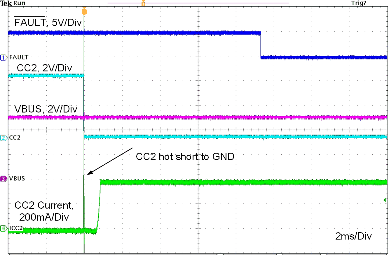
CC1 = Rd CC2 = Ra
Figure 11-34 CC2 Hot Short to GND
GUID-B8119C90-6CF8-4A77-8F10-3E7817549BE9-low.gif
CC1 = Rd CC2 = OPEN NO LOAD
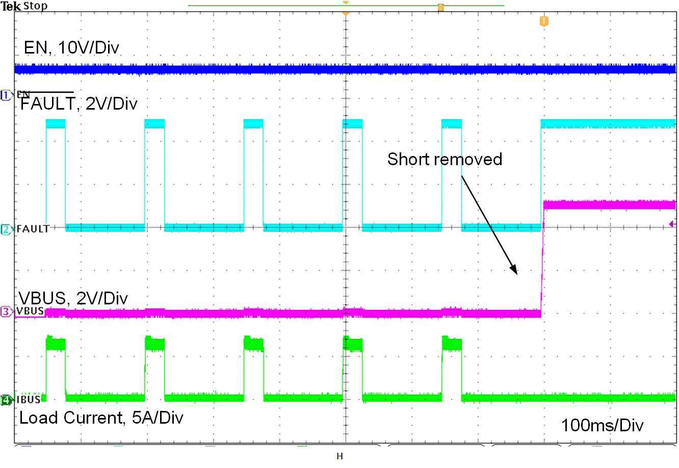
Figure 11-36 VBUS Short to BAT Recovery With External FET
GUID-262EC263-7B36-4314-91A2-39D7F827EF18-low.gif
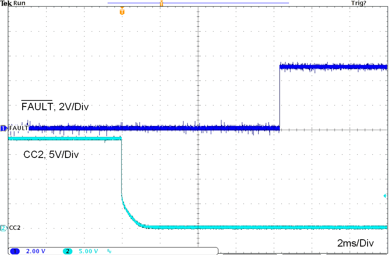
CC1 = Rd CC2 = OPEN NO LOAD
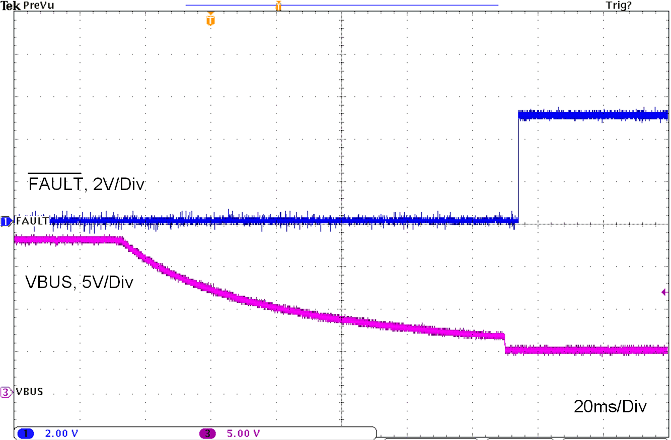
Figure 11-38 CC Short to BAT Recovery
GUID-DED69AE0-0E77-4D98-AEF2-04EB27701B13-low.gif
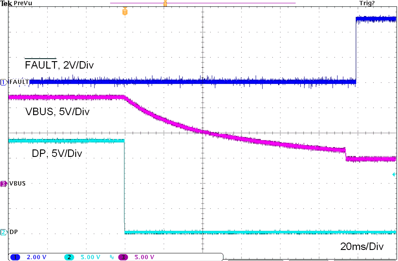
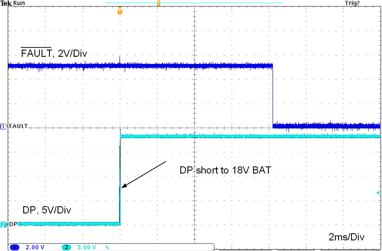
CC1 = Rd CC2 = OPEN NO LOAD
Figure 11-40 DP Short to BAT Recovery
GUID-77D1BF1A-E7DE-4513-95C0-F83B7AD60635-low.gif
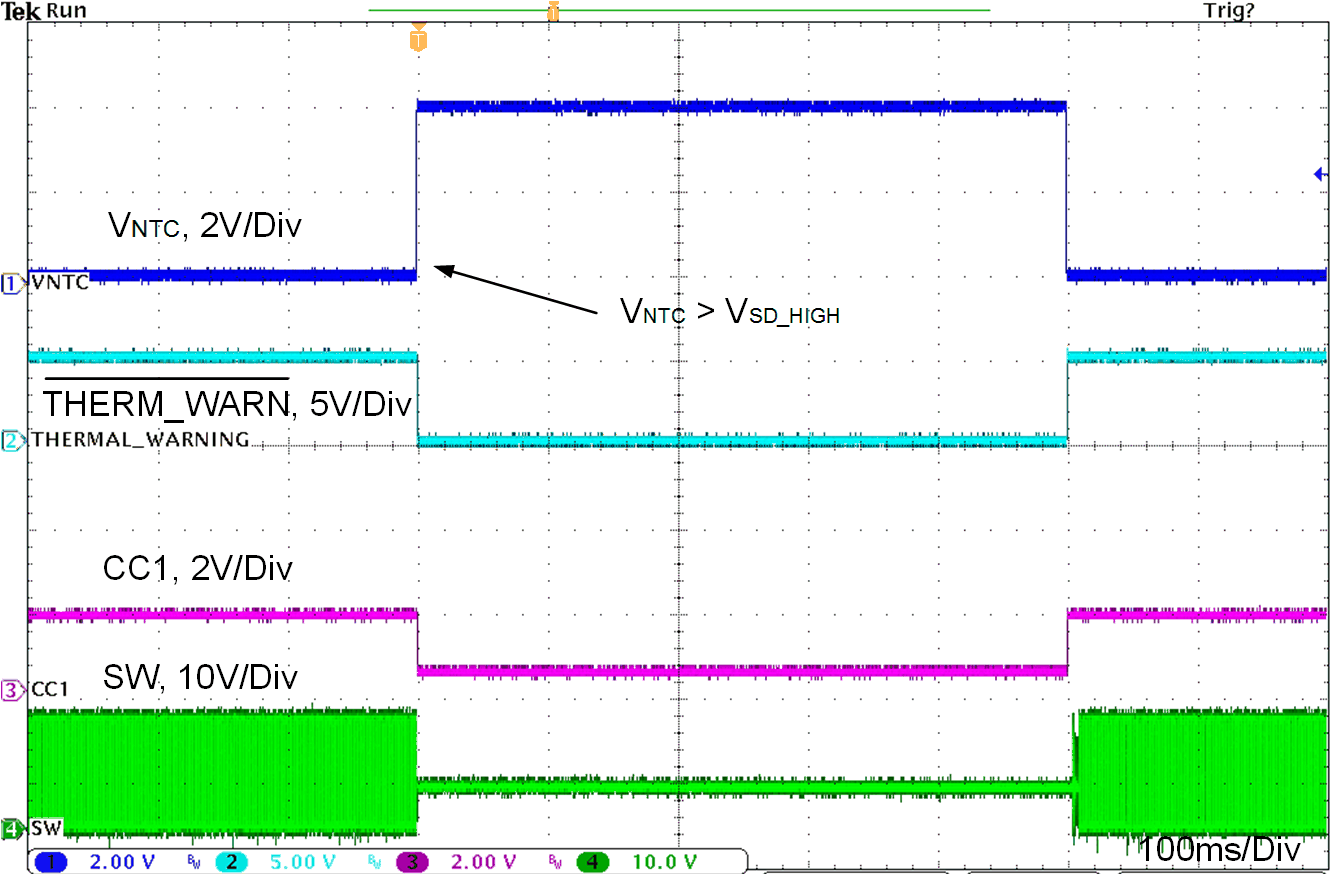
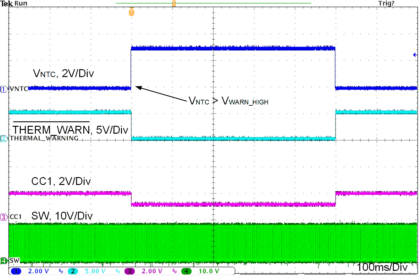
VNTC = 0 V to 4 V CC1 = Rd CC2 = OPEN
Figure 11-42 Thermal Sensing with NTC Behavior 2
GUID-20210504-CA0I-VRZJ-47LF-HKGWM4BBHJD6-low.gif
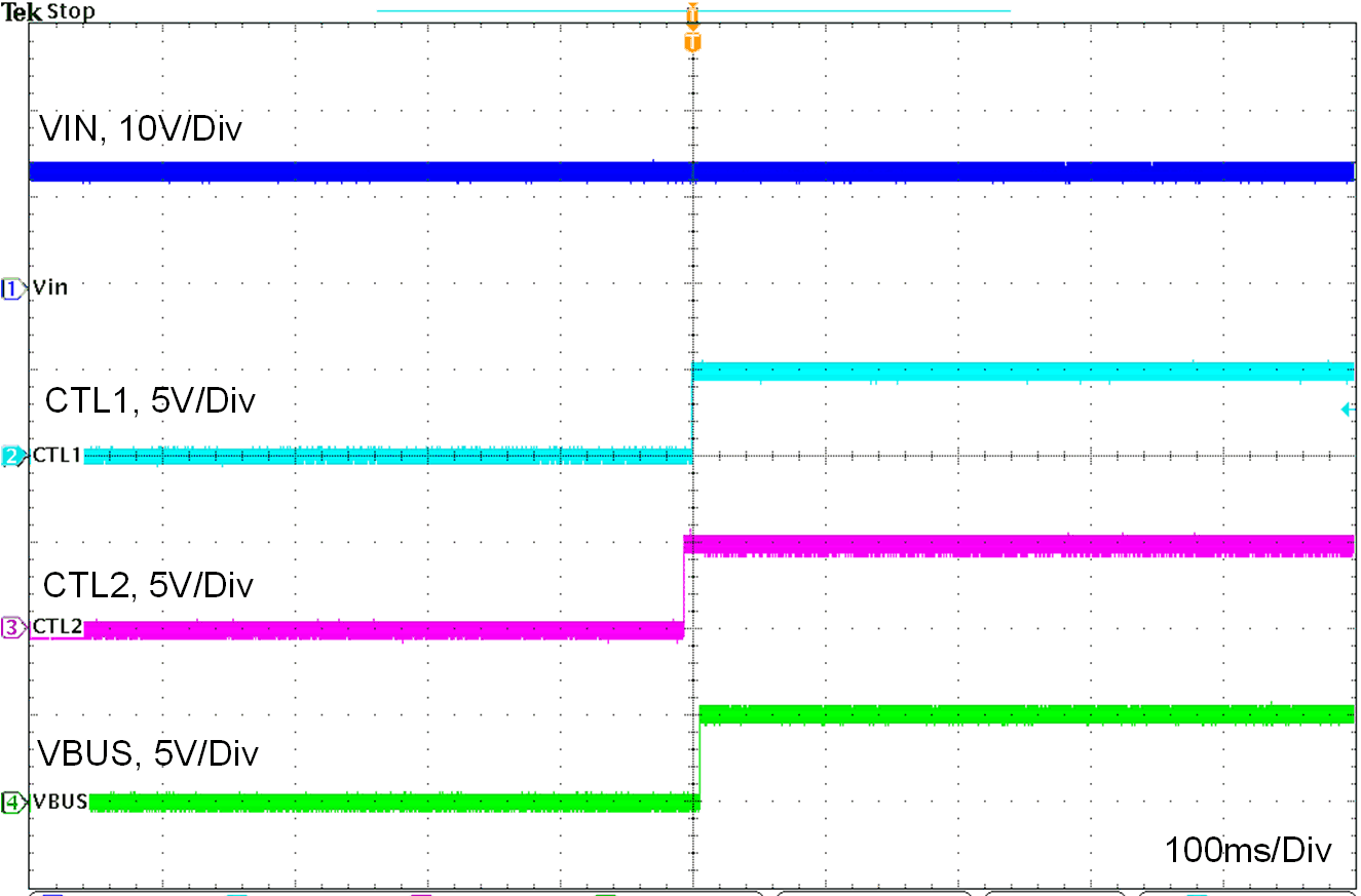
VIN13.5 V CC1 = Rd CTRL12 = 00 to 11
Figure 11-44 Client Mode to CDP Mode
GUID-2DFF53F8-E84E-4E46-AC81-5239B3010DC9-low.gif
VOUT = 5.1 V fSW = 2100 kHz L = 3.3 uH
Figure 11-3 Buck Only Efficiency
GUID-4EB9BC1B-B5FC-4F3D-8758-6EA1272C89C0-low.gif
RSENS = 15 mΩ fSW = 2100 kHz L = 3.3uH
Figure 11-5 Efficiency With Sense Resistor
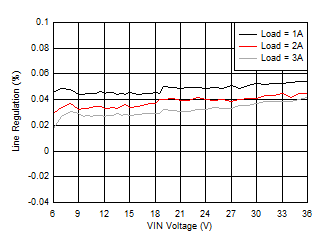
GUID-3A30FBCA-F35B-4435-B3E7-E1651DE389A8-low.gif
VOUT = 5.1 V fSW = 400 kHz
Figure 11-7 Line Regulation
GUID-DAA83397-5B70-4E62-8BB5-BB9F4B2FC1CA-low.gif
ILOAD = 0.75 A to 2.25 A RIMON = 0 Ω
Figure 11-9 Load Transient Without Cable Compensation
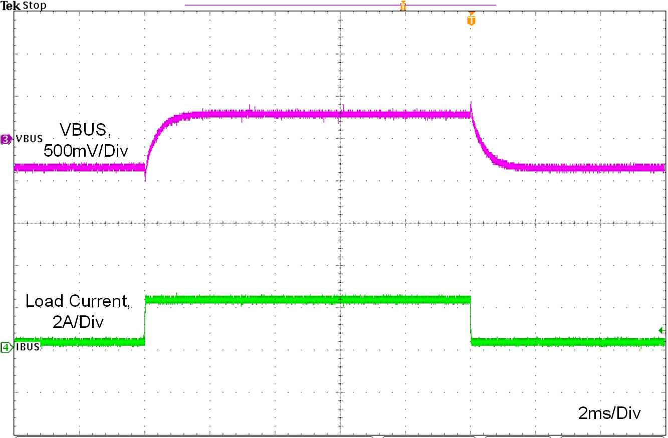
GUID-FD4F8E64-3DB2-4A05-8979-3A5372393C09-low.gif
ILOAD = 0.75 A to 2.25 A RIMON = 13 kΩ
Figure 11-11 Load Transient with Cable Compensation
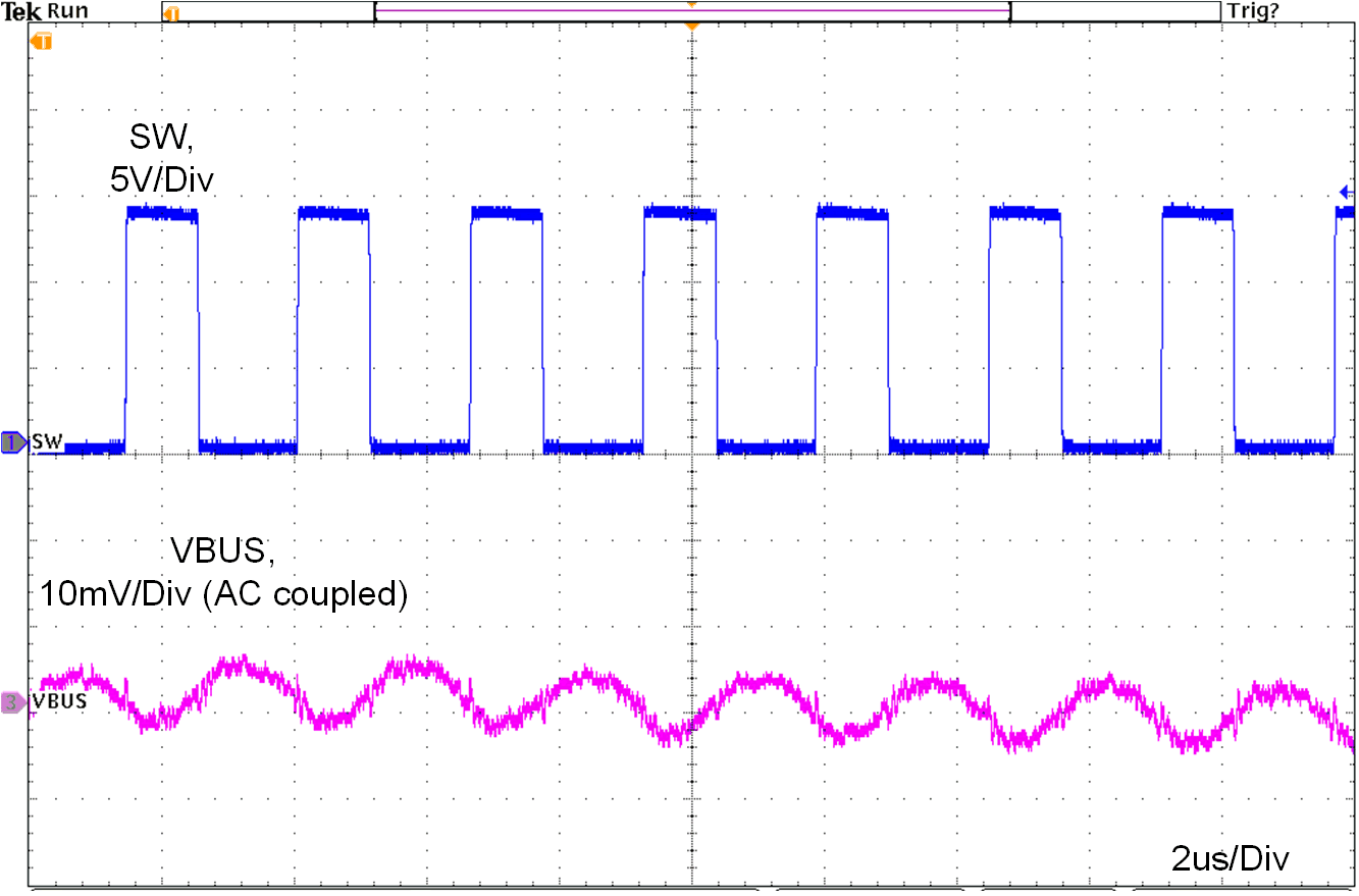
GUID-92040EB7-0CFD-42B9-8545-6F7BA765CE43-low.gif
RIMON = 13 kΩ
Figure 11-13 3.5-A Output Ripple
GUID-D1E91B3E-5111-47D4-95B7-63DF15278C51-low.gif
RIMON = 13 kΩ
Figure 11-15 No Load Output Ripple
GUID-A5948AA3-4ADA-4E73-95C1-035EB92C3F83-low.gif
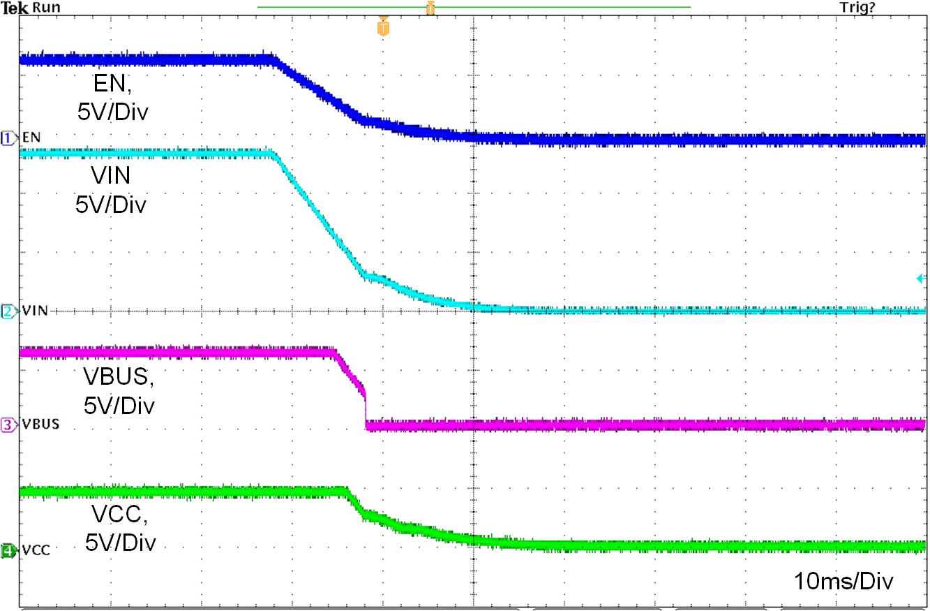
VIN = 13.5 V to 0 V CC1 = Rd ILOAD = 3 A
Figure 11-17 Shutdown Relate to VIN
GUID-7D09FEA0-053F-4561-8ADA-399D8BE05906-low.gif
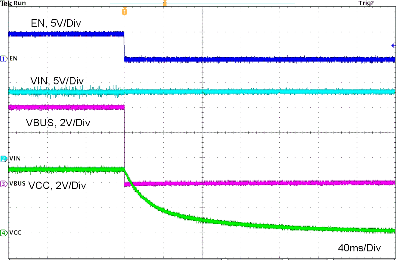
EN = 5 V to 0 V CC1 = Rd ILOAD = 3 A
Figure 11-19 Shutdown Relate to EN
GUID-3AAE8407-BC38-4177-BC7C-73BED7D4A3DF-low.gif
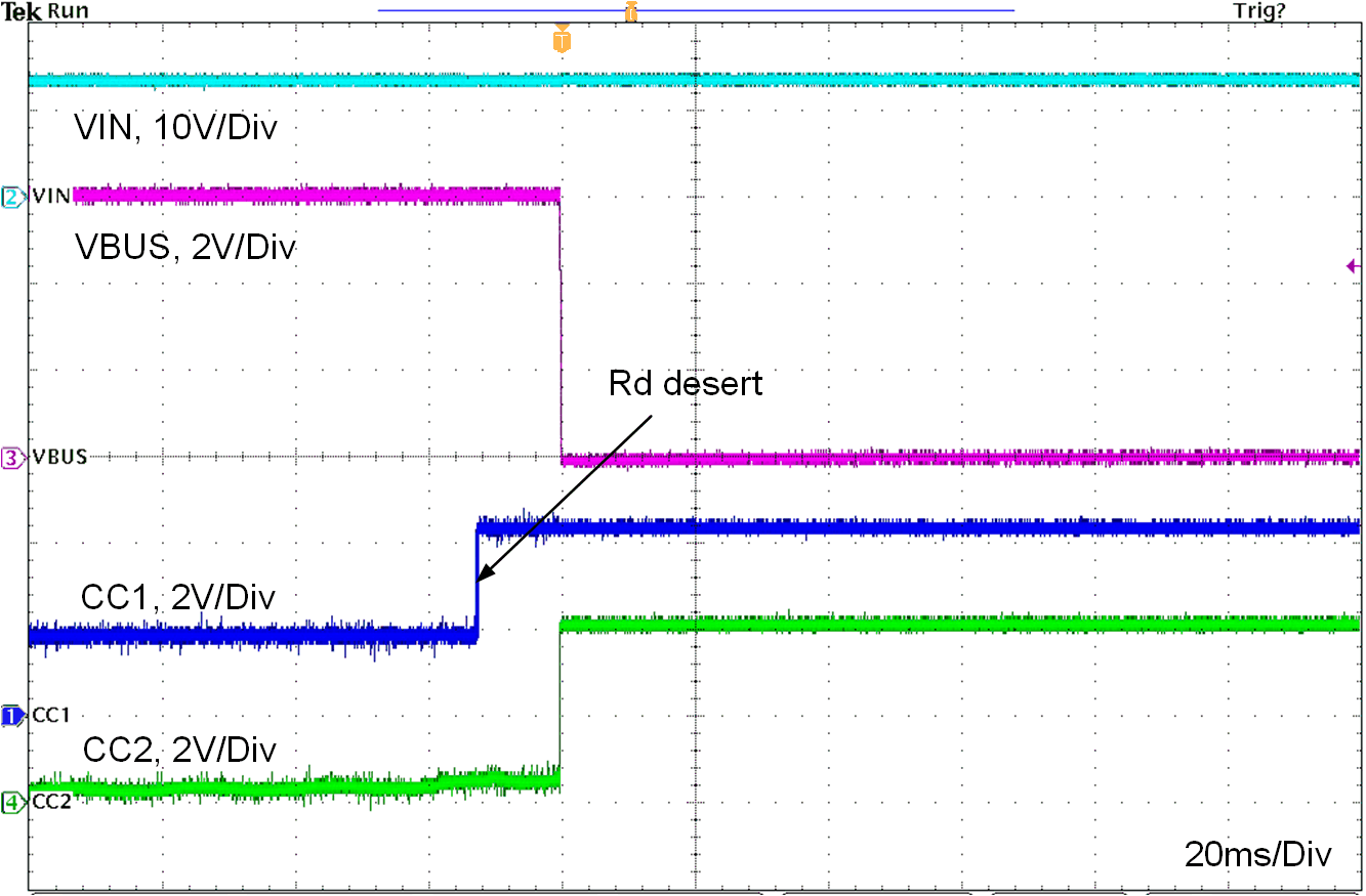
CC1 = Rd to Open CC2 = Open ILOAD = 3 A
Figure 11-21 Rd Desert
GUID-20210504-CA0I-N71X-CWWL-SD9HHHSKKJXT-low.gif
RLIMIT = 13 kΩ
Figure 11-23 Short Circuit Recovery Without External FET
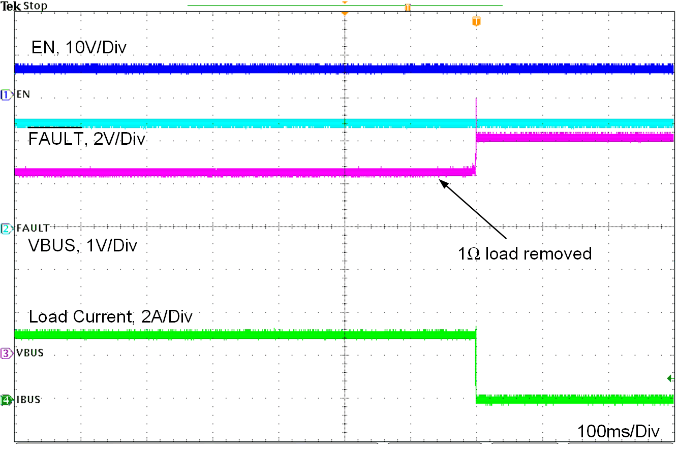
GUID-20210504-CA0I-DHLF-HDG3-QRFKRGX6JKGD-low.gif
RLIMIT = 13 kΩ
Figure 11-25 1-Ω Load Recovery Without External FET
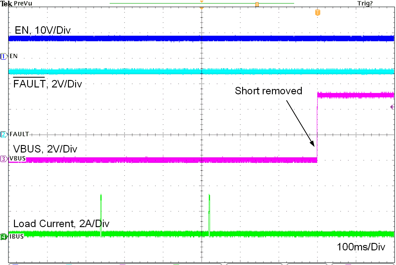
GUID-20210504-CA0I-72PK-HWXT-V8473CV5HNK9-low.gif
RLIMIT = 6.8 kΩ
Figure 11-27 Short Circuit Recovery With External FET
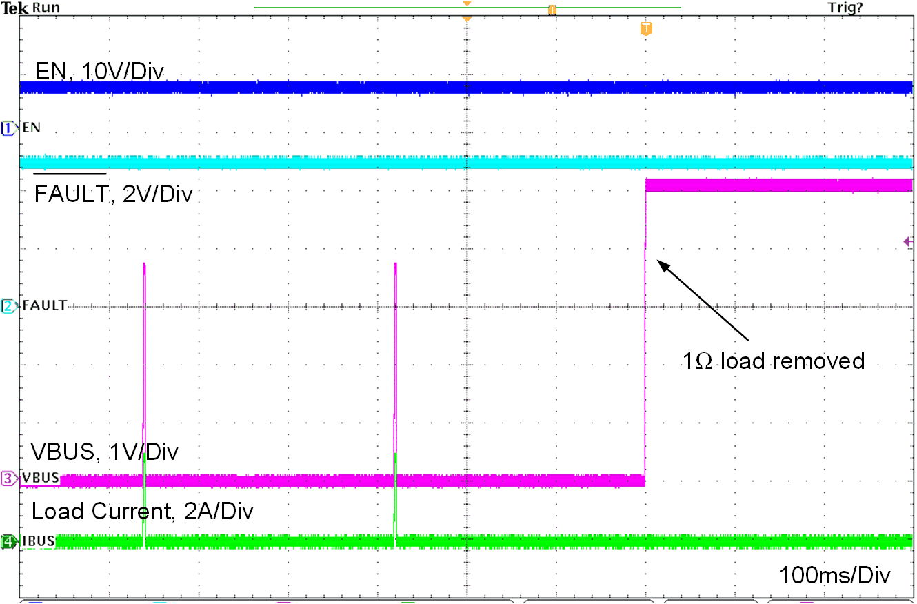
GUID-20210504-CA0I-TKZJ-TR25-NXJMKXLQJDGT-low.gif
RLIMIT = 6.8 kΩ
Figure 11-29 1-Ω Load Recovery With External FET
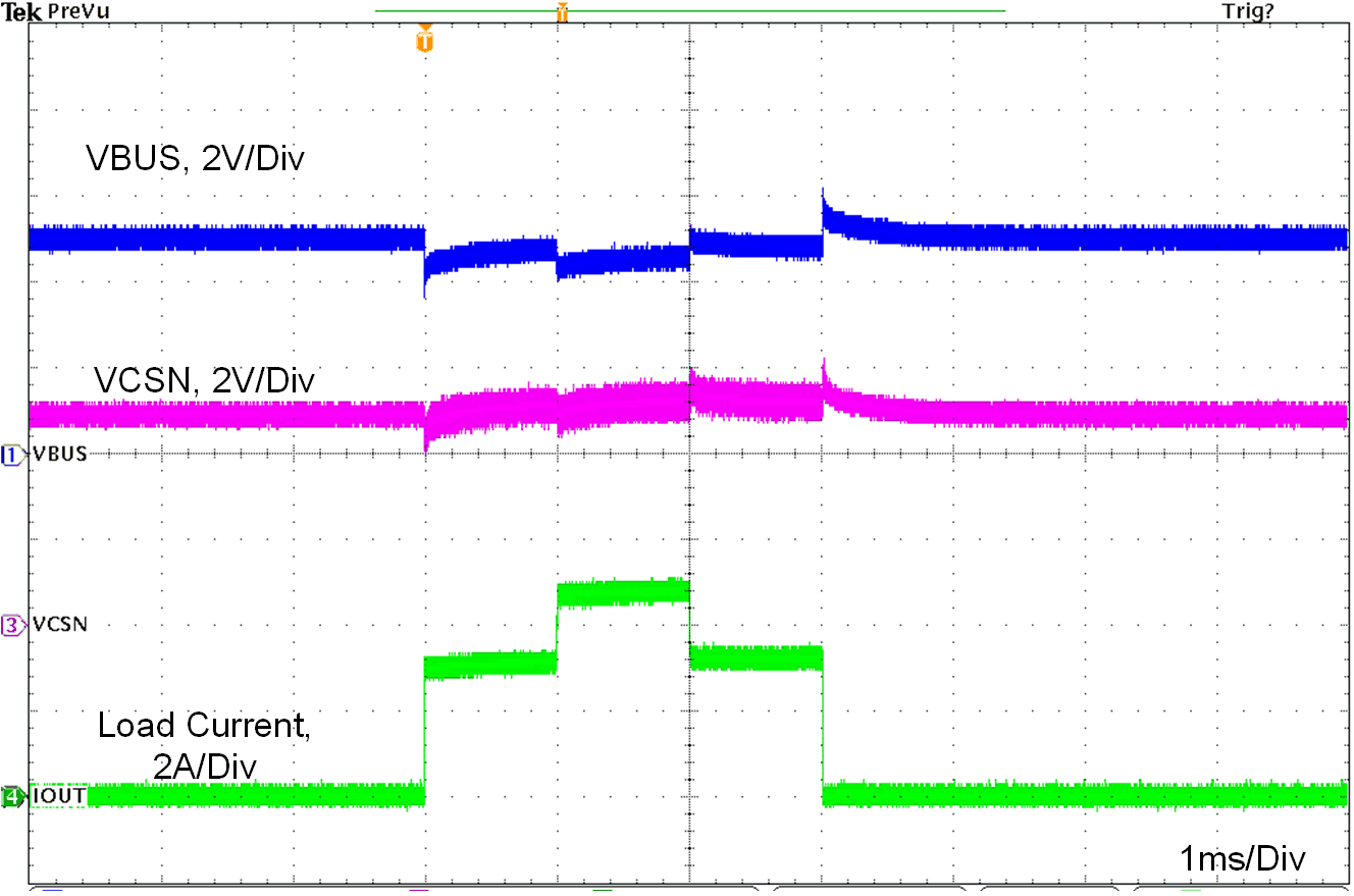
GUID-20210504-CA0I-PSM4-PLCD-PRXKPRZ3QPJ7-low.gif
ILOAD1 = 3 A ILOAD2 = 4.8 A RLIMIT = 6.8 kΩ
Figure 11-31 MFI Over-Current Test With External FET
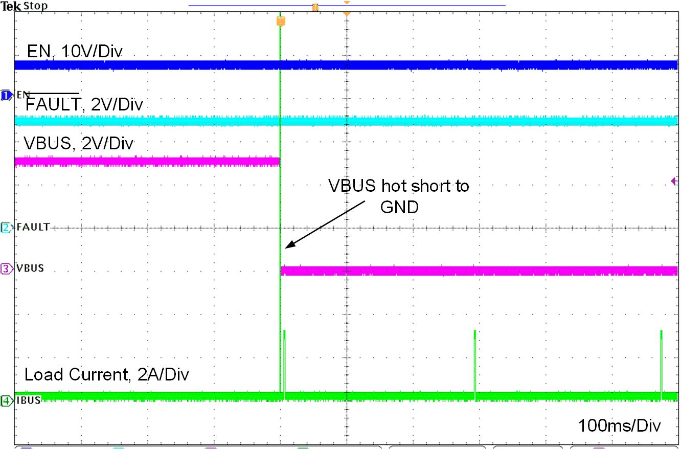
GUID-20210504-CA0I-RH5J-SLJH-7DPBFCNSPDSS-low.gif
RLIMIT = 6.8 kΩ
Figure 11-33 VBUS Hot Short to GND with External FET
GUID-6074A81B-217A-47AA-9F4A-7652FF8E7DB3-low.gif
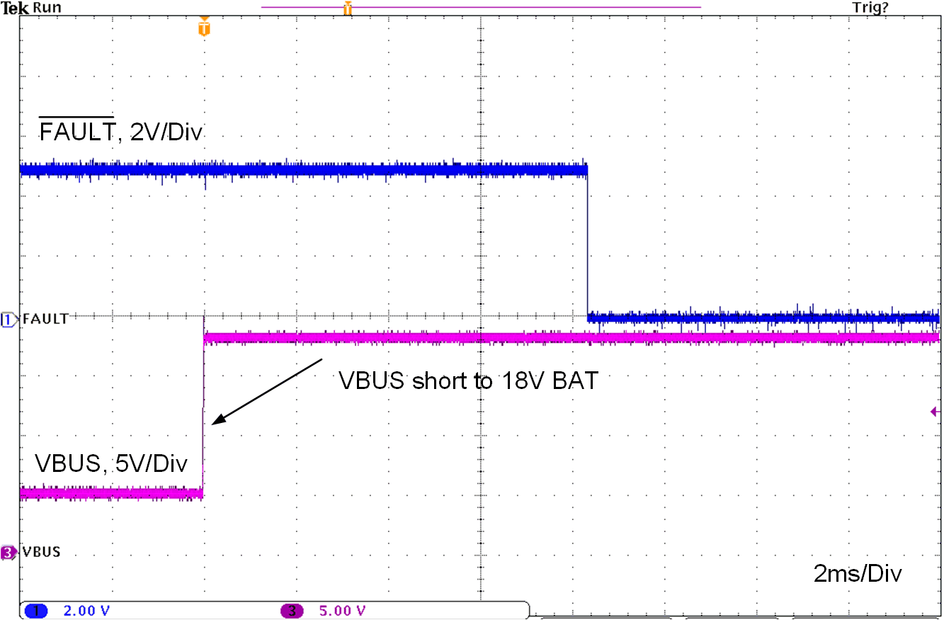
CC1 = Rd CC2 = OPEN NO LOAD
Figure 11-35 VBUS Short to BAT with External FET
GUID-96C26FE5-1806-4BA7-B640-5E7FB2207E91-low.gif
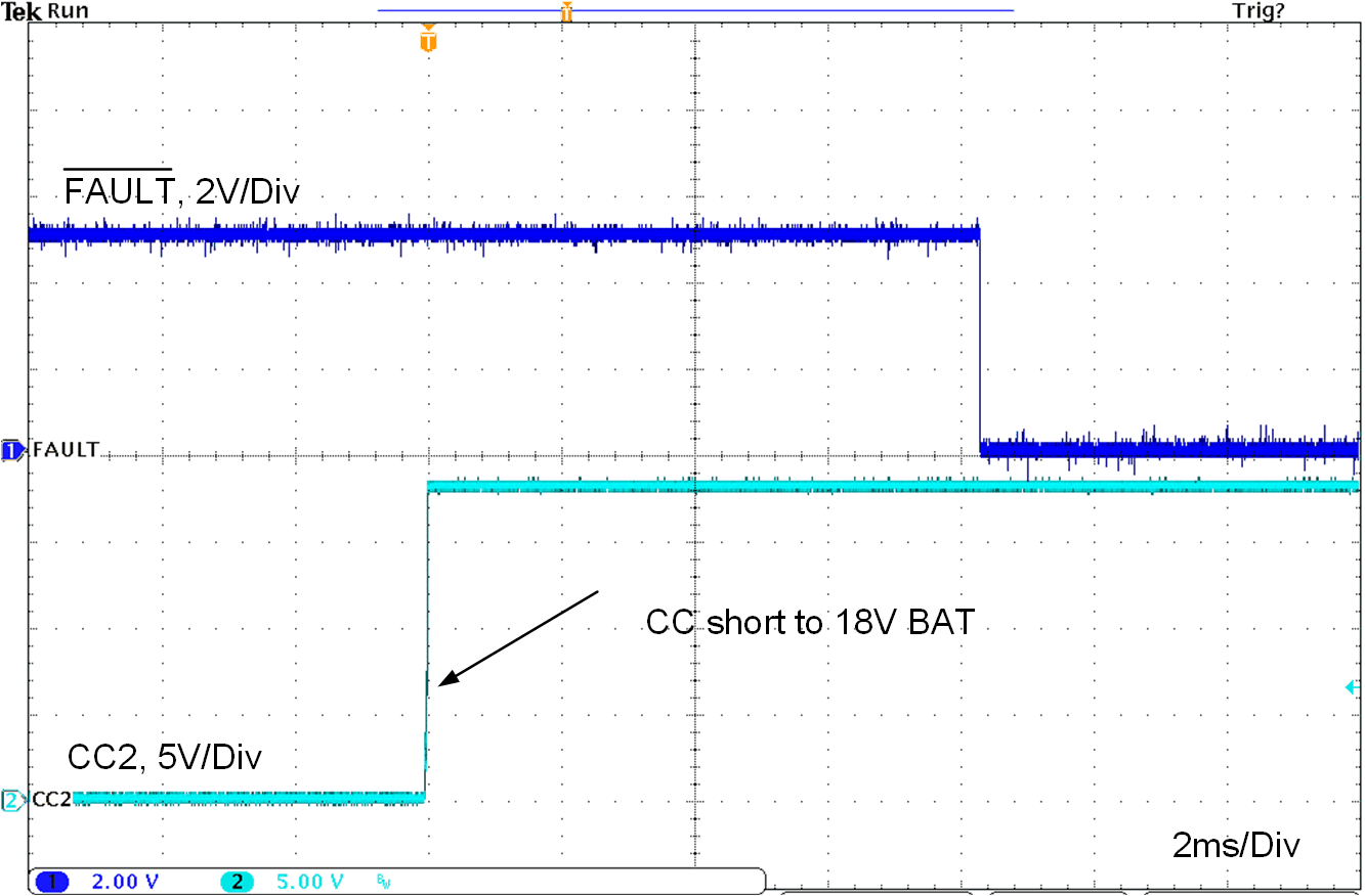
CC1 = Rd CC2 = OPEN NO LOAD
Figure 11-37 CC Short to BAT
GUID-37458533-58F1-4D60-9D01-06A00283F45A-low.gif
CC1 = Rd CC2 = OPEN NO LOAD
Figure 11-39 DP Short to BAT
GUID-3B229445-A3BE-42F9-A636-E54E6E653B3F-low.gif
VNTC = 0 V to 3 V CC1 = Rd CC2 = OPEN
Figure 11-41 Thermal Sensing with NTC Behavior 1
GUID-20210504-CA0I-G7GP-Z9HJ-HGB6XXD4CVDL-low.gif
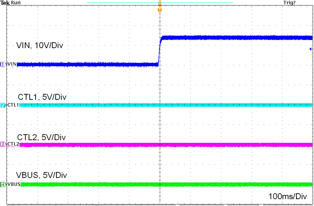
VIN = 0 V to 13.5 V CC1 = Rd CTRL12 = 00
Figure 11-43 Client mode Startup