JAJSF04C June   2017  – April 2018 TPS2595

PRODUCTION DATA.  

  1. 特長
  2. アプリケーション
  3. 概要
    1.     Device Images
      1.      概略回路図
      2.      TPS25953x過電圧クランプの応答時間
  4. 改訂履歴
  5. Device Comparison Table
  6. Pin Configuration and Functions
    1.     Pin Functions
  7. Specifications
    1. 7.1 Absolute Maximum Ratings
    2. 7.2 ESD Ratings
    3. 7.3 Recommended Operating Conditions
    4. 7.4 Thermal Information
    5. 7.5 Electrical Characteristics
    6. 7.6 Switching Characteristics
    7. 7.7 Typical Characteristics
  8. Detailed Description
    1. 8.1 Overview
    2. 8.2 Functional Block Diagram
    3. 8.3 Feature Description
      1. 8.3.1 Undervoltage Protection (UVP) and Undervoltage Lockout (UVLO)
      2. 8.3.2 Overvoltage Protection
        1. 8.3.2.1 Overvoltage Lockout (OVLO)
        2. 8.3.2.2 Overvoltage Clamp (OVC)
      3. 8.3.3 Inrush Current, Overcurrent and Short Circuit Protection
        1. 8.3.3.1 Slew Rate and Inrush Current Control (dVdt)
        2. 8.3.3.2 Active Current Limiting
        3. 8.3.3.3 Short Circuit Protection
      4. 8.3.4 Overtemperature Protection (OTP)
      5. 8.3.5 Fault Indication (FLT )
      6. 8.3.6 Quick Output Discharge (QOD)
    4. 8.4 Device Functional Modes
      1. 8.4.1 Enable and Fault Pin Functional Mode 1: Single Device, Self-Controlled
      2. 8.4.2 Enable and Fault Pin Functional Mode 2: Single Device, Host-Controlled
      3. 8.4.3 Enable and Fault Pin Functional Mode 2: Multiple Devices, Self-Controlled
  9. Application and Implementation
    1. 9.1 Application Information
    2. 9.2 Typical Application
      1. 9.2.1 Design Requirements
      2. 9.2.2 Detailed Design Procedure
        1. 9.2.2.1 Programming the Current-Limit Threshold: RILM Selection
        2. 9.2.2.2 Undervoltage Lockout Set Point
        3. 9.2.2.3 Setting Output Voltage Ramp Time (TdVdT)
          1. 9.2.2.3.1 Case 1: Start-Up Without Load. Only Output Capacitance COUT Draws Current
          2. 9.2.2.3.2 Case 2: Start-Up With Load. Output Capacitance COUT and Load Draw Current
      3. 9.2.3 Support Component Selection: CIN
      4. 9.2.4 Application Curves
      5. 9.2.5 Controlled Power Down (Quick Output Discharge) using TPS2595x5
      6. 9.2.6 Overvoltage Lockout using TPS259573
  10. 10Power Supply Recommendations
    1. 10.1 Transient Protection
    2. 10.2 Output Short-Circuit Measurements
  11. 11Layout
    1. 11.1 Layout Guidelines
    2. 11.2 Layout Example
  12. 12デバイスおよびドキュメントのサポート
    1. 12.1 ドキュメントのサポート
      1. 12.1.1 関連資料
      2. 12.1.2 関連リンク
    2. 12.2 ドキュメントの更新通知を受け取る方法
    3. 12.3 コミュニティ・リソース
    4. 12.4 商標
    5. 12.5 静電気放電に関する注意事項
    6. 12.6 Glossary
  13. 13メカニカル、パッケージ、および注文情報

パッケージ・オプション

メカニカル・データ(パッケージ|ピン)
サーマルパッド・メカニカル・データ
発注情報

Active Current Limiting

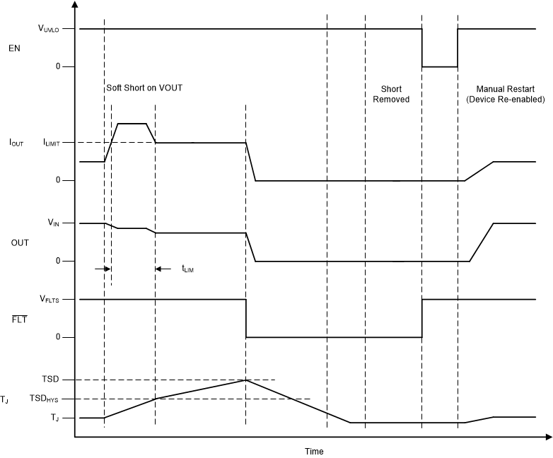
The load current is monitored during start-up and normal operation. When the load current exceeds the current limit trip point ILIMIT programmed by RILM resistor, the device regulates the current to the set limit ILIMIT within tLIM. The device exits current limiting when the load current falls below limit. Equation 4 can be used to find the RILM value for a desired current limit.

Equation 4. TPS2595 tps2595xx-equation-4.gif

In the current limiting state, the output voltage drops resulting in increased power dissipation in the internal FET leading to a thermal shutdown if the condition persists for an extended period of time. In this case, the device either stays latched-off or starts an auto retry cycle as explained in the Overtemperature Protection (OTP) section.
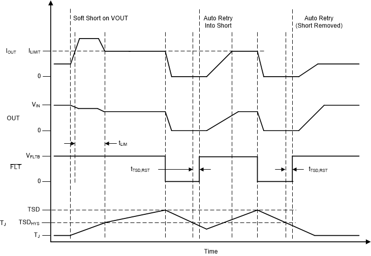
TPS2595 ILIM-Retry.gifFigure 50. TPS2595x1, TPS2595x3, TPS2595x5 Overcurrent Response (Auto-Retry)
TPS2595 ILIM-Latch.gifFigure 51. TPS2595x0 Overcurrent Response (Latch-Off)