JAJSCA1A June   2016  – September 2016 TPS3779-Q1 , TPS3780-Q1

PRODUCTION DATA.  

  1. 特長
  2. アプリケーション
  3. 概要
  4. 改訂履歴
  5. Device Comparison Table
  6. Pin Configuration and Functions
  7. Specifications
    1. 7.1 Absolute Maximum Ratings
    2. 7.2 ESD Ratings
    3. 7.3 Recommended Operating Conditions
    4. 7.4 Thermal Information
    5. 7.5 Electrical Characteristics
    6. 7.6 Timing Requirements
    7. 7.7 Typical Characteristics
  8. Detailed Description
    1. 8.1 Overview
    2. 8.2 Functional Block Diagrams
    3. 8.3 Feature Description
      1. 8.3.1 Inputs (SENSE1, SENSE2)
      2. 8.3.2 Outputs (OUT1, OUT2)
    4. 8.4 Device Functional Modes
      1. 8.4.1 Normal Operation (VDD ≥ VDD(min))
      2. 8.4.2 Power-On-Reset (VDD < V(POR))
  9. Application and Implementation
    1. 9.1 Application Information
      1. 9.1.1 Threshold Overdrive
      2. 9.1.2 Sense Resistor Divider
    2. 9.2 Typical Applications
      1. 9.2.1 Monitoring Two Separate Rails
        1. 9.2.1.1 Design Requirements
        2. 9.2.1.2 Detailed Design Procedure
        3. 9.2.1.3 Application Curve
      2. 9.2.2 Early Warning Detection
        1. 9.2.2.1 Design Requirements
        2. 9.2.2.2 Detailed Design Procedure
        3. 9.2.2.3 Application Curve
  10. 10Power-Supply Recommendations
  11. 11Layout
    1. 11.1 Layout Guidelines
    2. 11.2 Layout Example
  12. 12デバイスおよびドキュメントのサポート
    1. 12.1 デバイス・サポート
      1. 12.1.1 開発サポート
        1. 12.1.1.1 評価モジュール
        2. 12.1.1.2 SPICEモデル
      2. 12.1.2 デバイスの項目表記
    2. 12.2 ドキュメントのサポート
      1. 12.2.1 関連資料
    3. 12.3 ドキュメントの更新通知を受け取る方法
    4. 12.4 関連リンク
    5. 12.5 コミュニティ・リソース
    6. 12.6 商標
    7. 12.7 静電気放電に関する注意事項
    8. 12.8 Glossary
  13. 13メカニカル、パッケージ、および注文情報

パッケージ・オプション

メカニカル・データ(パッケージ|ピン)
サーマルパッド・メカニカル・データ
発注情報

Layout

Layout Guidelines

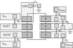
Place the VDD decoupling capacitor close to the device.

Avoid using long traces for the VDD supply node. The VDD capacitor, along with parasitic inductance from the supply to the capacitor, can form an LC tank circuit that creates ringing with peak voltages above the maximum VDD voltage.

Layout Example

TPS3779-Q1 TPS3780-Q1 dbv_lay_sbvs273.gif Figure 26. Example SOT-23 Layout