SBVS302 November 2016 TPS3852
PRODUCTION DATA.
- 1 Features
- 2 Applications
- 3 Description
- 4 Revision History
- 5 Pin Configuration and Functions
- 6 Specifications
- 7 Detailed Description
- 8 Application and Implementation
- 9 Power Supply Recommendations
- 10Layout
- 11Device and Documentation Support
- 12Mechanical, Packaging, and Orderable Information
パッケージ・オプション
メカニカル・データ(パッケージ|ピン)
- DRB|8
サーマルパッド・メカニカル・データ
- DRB|8
発注情報
1 Features
- VDD Input Voltage Range: 1.6 V to 6.5 V
- 0.8% Voltage Threshold Accuracy
- Low Supply Current: IDD = 10 µA (typical)
- User-Programmable Watchdog Timeout
- Factory Programmed Precision Watchdog and Reset Timers:
- ±15% Accurate WDT and RST Delays
- Open-Drain Outputs
- Manual Reset Input (MR)
- Precision Undervoltage Monitoring
- Supports Common Rails from 1.8 V to 5 V
- 4% and 7% Thresholds Available
- 0.5% Hysteresis
- Watchdog Disable Feature
- Available in a Small 3-mm × 3-mm, 8-Pin VSON Package
2 Applications
- Safety Critical Applications
- Telematics Control Units
- High-Reliability Industrial Systems
- Patient Monitoring
- Industrial Control Systems
- FPGAs and ASICs
- Microcontrollers and DSPs
3 Description
The TPS3852 is a precision voltage supervisor with an integrated window watchdog timer. The TPS3852 includes a precision undervoltage supervisor with an undervoltage threshold (VITN) that achieves 0.8% accuracy over the specified temperature range of –40°C to +125°C. In addition, the TPS3852 includes accurate hysteresis making the device ideal for use with tight tolerance systems. The supervisor RESET delay features a 15% accuracy, high-precision delay timer.
The TPS3852 includes a programmable window watchdog timer for a wide variety of applications. The dedicated watchdog output (WDO) enables increased resolution to help determine the nature of fault conditions. The watchdog timeouts can be programmed either by an external capacitor, or by factory-programmed default delay settings. The watchdog can be disabled to avoid undesired watchdog timeouts during the development process.
The TPS3852 is available in a small 3.00-mm × 3.00-mm, 8-pin VSON package.
Device Information(1)
| PART NUMBER | PACKAGE | BODY SIZE (NOM) |
|---|---|---|
| TPS3852 | VSON (8) | 3.00 mm × 3.00 mm |
- For all available packages, see the orderable addendum at the end of the data sheet.
Space
Space
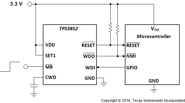
Typical Application Circuit

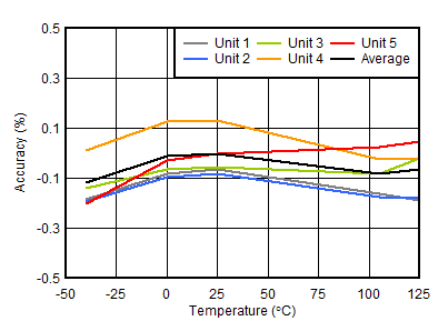
Undervoltage Threshold (VITN) Accuracy vs Temperature
