SBVS302 November 2016 TPS3852
PRODUCTION DATA.
- 1 Features
- 2 Applications
- 3 Description
- 4 Revision History
- 5 Pin Configuration and Functions
- 6 Specifications
- 7 Detailed Description
- 8 Application and Implementation
- 9 Power Supply Recommendations
- 10Layout
- 11Device and Documentation Support
- 12Mechanical, Packaging, and Orderable Information
パッケージ・オプション
メカニカル・データ(パッケージ|ピン)
- DRB|8
サーマルパッド・メカニカル・データ
- DRB|8
発注情報
7 Detailed Description
7.1 Overview
The TPS3852 is a high-accuracy voltage supervisor with an integrated window watchdog timer. This device includes a precision undervoltage supervisor with a threshold that achieves 0.8% accuracy over the specified temperature range of –40°C to +125°C. In addition, the TPS3852 includes accurate hysteresis on the threshold, making the device ideal for use with tight tolerance systems where voltage supervisors must ensure a RESET before the minimum supply tolerance of the microprocessor or system-on-a-chip (SoC) is reached.
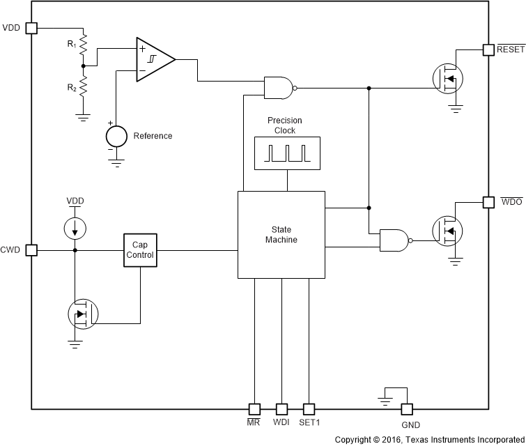
7.2 Functional Block Diagram

7.3 Feature Description
7.3.1 RESET
Connect RESET to VPU through a 1-kΩ to 100-kΩ pullup resistor. RESET remains high (deasserted) when VDD is greater than the negative threshold voltage (VITN). If VDD falls below the negative threshold (VITN), then RESET is asserted, driving the RESET pin to low impedance. When VDD rises above VITN + VHYST, a delay circuit is enabled that holds RESET low for a specified reset delay period (tRST). When the reset delay has elapsed, the RESET pin goes to a high-impedance state and uses a pullup resistor to hold RESET high. The pullup resistor must be connected to the desired voltage rail to allow other devices to be connected at the correct interface voltage. To ensure proper voltage levels, give some consideration when choosing the pullup resistor values. The pullup resistor value is determined by output logic low voltage (VOL), leakage current (ID), and the current through the RESET pin IRESET.
7.3.2 Manual Reset MR
The manual reset (MR) input allows a processor or other logic circuits to initiate a reset. A logic low on MR causes RESET to assert. After MR returns to a logic high and VDD is above VITN + VHYST, RESET is deasserted after the reset delay time (tRST). If MR is not controlled externally, then MR can either be connected to VDD or left floating because the MR pin is internally pulled up. When MR is asserted, the watchdog is disabled and all signals input to WDI are ignored.
7.3.3 UV Fault Detection
The TPS3852 features undervoltage detection for common rails between 1.8 V and 5 V. The voltage is monitored on the input rail of the device. If VDD drops below VITN, then RESET is asserted (driven low). When VDD is above VITN + VHYST, RESET deasserts after tRST, as shown in Figure 16. The internal comparator has built-in hysteresis that provides some noise immunity and ensures stable operation. Although not required in most cases, for noisy applications, good analog design practice is to place a 1-nF to 100-nF bypass capacitor close to the VDD pin to reduce sensitivity to transient voltages on the monitored signal.
 Figure 16. Undervoltage Detection
7.3.4 Watchdog Mode
This section provides information for the watchdog mode of operation.
7.3.4.1 SET1
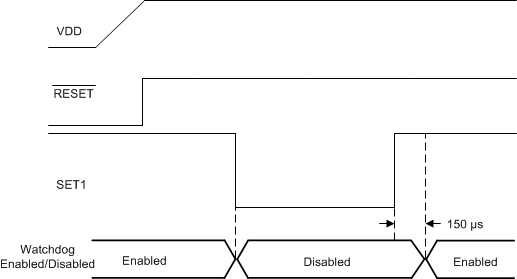
The SET1 pin can enable and disable the watchdog timer. If SET1 is set to GND, the watchdog timer is disabled and WDI is ignored. When the watchdog is disabled WDO will be in a high impedance state. If the watchdog timer is disabled, drive the WDI pin to either GND or VDD to ensure that there is no increase in IDD. When SET1 is logic high, the watchdog operates normally. The SET1 pin can be changed dynamically; however, if the watchdog is going from disabled to enabled there is a setup time tWD-setup where the watchdog does not respond to changes on WDI, as shown in Figure 17.
 Figure 17. Enabling and Disabling the Watchdog
7.3.4.2 Window Watchdog Timer
This section provides information for the window watchdog mode of operation. A window watchdog is typically employed in safety critical applications where a traditional watchdog timer is inadequate. In a traditional watchdog there is a maximum time in which a pulse must be issued to prevent the reset from occurring. In a window watchdog the pulse must be issued between a maximum lower window time (tWDL(max)) and the minimum upper window time (tWDU(min)) set by the CWD pin.
7.3.4.3 Watchdog Input WDI
WDI is the watchdog timer input that controls the WDO output. The WDI input is triggered by the falling edge of the input signal. For the first pulse, the watchdog acts as a traditional watchdog timer; thus, the first pulse must be issued before tWDU(min). After the first pulse, to ensure proper functionality of the watchdog timer, always issue the WDI pulse within the window of tWDL(max) and tWDU(min). If the pulse is issued in this region, then WDO remains unasserted. Otherwise, the device asserts WDO, putting the WDO pin into a low-impedance state.
The watchdog input (WDI) is a digital pin. In order to ensure there is no increase in IDD, drive the WDI pin to either VDD or GND at all times. Putting the pin to an intermediate voltage can cause an increase in supply current (IDD) because of the architecture of the digital logic gates. When RESET is asserted, the watchdog is disabled and all signals input to WDI are ignored. When RESET is no longer asserted, the device resumes normal operation and no longer ignores the signal on WDI. If the watchdog is disabled, drive the WDI pin to either VDD or GND.
7.3.4.4 CWD
The CWD pin provides the user the functionality of both high precision factory programmed window watchdog timing options and user programmable window watchdog timing. The CWD pin can be either pulled-up to VDD through a resistor, have an external capacitor to ground, or be left floating. Every time that the part issues a reset event and the supply voltage is above VITN the part will try to determine, which of these three options is connected to the pin. There is an internal state machine that the device goes through to determine which option is connected to the CWD pin. The state machine can take up to 381 μs to determine if the CWD pin is left floating, pulled-up through a resistor, or connected to a capacitor.
If the CWD pin is being pulled up to VDD using a pull-up resistor then a 10-kΩ resistor should be used.
7.3.4.5 Watchdog Output WDO
The TPS3852 features a window watchdog with an independent watchdog output (WDO). The independent watchdog output gives the flexibility to flag when there is a fault in the watchdog timing without performing an entire system reset. For legacy applications WDO can be tied to RESET. While the RESET output is not asserted the WDO signal will maintain normal operation. However, when the RESET signal is asserted the WDO pin will go into a high impedance state. This is due to using the standard RESET timing options when a fault occurs on WDO. Once RESET is unasserted the window watchdog timer will resume normal operation.
7.4 Device Functional Modes
Table 1 summarises the functional modes of TPS3852.
Table 1. Device Functional Modes
| VDD | WDI | WDO | RESET | ||
|---|---|---|---|---|---|
| VDD < VPOR | — | — | Undefined | ||
| VPOR ≤ VDD < VDD(min) | Ignored | High | Low | ||
| VDD(min) ≤ VDD ≤ VITN + VHYST(1) | Ignored | High | Low | ||
| VDD > VITN(2) | tWDL(max) < tPULSE < tWDU(min)(3) | High | High | ||
| tPULSE > tWDU(min)(3) | Low | High | |||
| tPULSE < tWDL(max)(3) | Low | High | |||
7.4.1 VDD is Below VPOR ( VDD < VPOR)
When VDD is less than VPOR, RESET is undefined and can be either high or low. The state of RESET largely depends on the load that the RESET pin is experiencing.
7.4.2 Above Power-On-Reset, But Less Than VDD(min) (VPOR ≤ VDD < VDD(min))
When the voltage on VDD is less than VDD(min), and greater than or equal to VPOR, the RESET signal is asserted (logic low). When RESET is asserted, the watchdog output WDO is in a high-impedance state regardless of the WDI signal that is input to the device.
7.4.3 Normal Operation (VDD ≥ VDD(min))
When VDD is greater than or equal to VDD(min), the RESET signal is determined by VDD. When RESET is asserted, WDO goes to a high-impedance state. WDO is then pulled high through the pullup resistor.