JAJS234H MARCH 2007 – May 2019 TPS40192 , TPS40193
PRODUCTION DATA.
- 1 特長
- 2 アプリケーション
- 3 概要
- 4 改訂履歴
- 5 概要(続き)
- 6 Pin Configuration and Functions
- 7 Specifications
- 8 Detailed Description
-
9 Application and Implementation
- 9.1 Application Information
- 9.2
Typical Application
- 9.2.1 Design Requirements
- 9.2.2
Detailed Design Procedure
- 9.2.2.1 Selecting the Switching Frequency
- 9.2.2.2 Inductor Selection
- 9.2.2.3 Output Capacitor Selection (C8)
- 9.2.2.4 Peak Current Rating of the Inductor
- 9.2.2.5 Input Capacitor Selection (C7)
- 9.2.2.6 MOSFET Switch Selection (Q1, Q2)
- 9.2.2.7 Boot Strap Capacitor
- 9.2.2.8 Input Bypass Capacitor (C6)
- 9.2.2.9 BP5 Bypass Capacitor (C5)
- 9.2.2.10 Input Voltage Filter Resistor (R11)
- 9.2.2.11 Short Circuit Protection (R9)
- 9.2.2.12 Feedback Compensation (Modeling the Power Stage)
- 9.2.2.13 Feedback Divider (R7, R8)
- 9.2.2.14 Error Amplifier Compensation (R6, R10, C1, C2, C3)
- 9.2.3 Application Curves
- 10Power Supply Recommendations
- 11Layout
- 12デバイスおよびドキュメントのサポート
- 13メカニカル、パッケージ、および注文情報
パッケージ・オプション
メカニカル・データ(パッケージ|ピン)
- DRC|10
サーマルパッド・メカニカル・データ
- DRC|10
発注情報
8.3.6 Selecting the Short Circuit Current
A short circuit in the devices is detected by sensing the voltage drop across the low-side MOSFET when it is on, and across the high-side MOSFET when it is on. If the voltage drop across either MOSFET exceeds the short circuit threshold in any given switching cycle, a counter increments one count. If the voltage across the high-side MOSFET was higher that the short circuit threshold, that MOSFET is turned off early. If the voltage drop across either MOSFET does not exceed the short circuit threshold during a cycle, the counter is decremented for that cycle. If the counter fills up (a count of 7) a fault condition is declared and the drivers turn off both MOSFETs. After a timeout of approximately 50 ms, the controller attempts to restart. If a short circuit is still present at the output, the current quickly ramps up to the short circuit threshold and another fault condition is declared and the process of waiting for the 50 ms an attempting to restart repeats. The low-side threshold increases as the low-side on time decreases due to blanking time and comparator response time. See Figure 11 for changes in the threshold as the low-side MOSFET conduction time decreases.
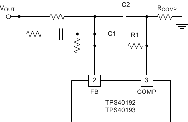
These devices provide three selectable short circuit protection thresholds for the low-side MOSFET: 100 mV, 200 mV and 280 mV. The particular threshold is selected by connecting a resistor from COMP to GND. Table 1 shows the short circuit thresholds for corresponding resistors from COMP to GND. When designing the compensation for the feedback loop, remember that a low impedance compensation network combined with a long network time constant can cause the short circuit threshold setting to not be as expected. The time constant and impedance of the network connected from COMP to FB should be as in Equation 1 to ensure no interaction with the short circuit threshold setting.

where
- t is 1 ms, the sampling time of the short circuit threshold setting circuit
- R1 and C1 are the values of the components in Figure 14
 Figure 14. Short Circuit Threshold Feedback Network
 Table 1. Short Circuit Threshold Voltage Selection
| COMPARATOR RESISTANCE
RCOMP (kΩ) |
CURRENT LIMIT THRESHOLD VOLTAGE (mV)
VILIM(V) |
|---|---|
| 12 ±10% | 280 |
| Open | 200 |
| 4 ±10% | 100 |
The range of short circuit current thresholds that can be expected is shown in Equation 2 and Equation 3.


where
- ISCP is the short circuit current
- VILIM is the short circuit threshold for the low-side MOSFET
- RDS(on) is the channel ON-resistance of the low-side MOSFET
Due to blanking time considerations, overcurrent threshold accuracy may fall off for duty cycle greater than 75% with the TPS40192, or 88% with the TPS40193. Specifically, the overcurrent comparator has only a very short time to sample the SW pin voltage under these conditions. As a result, the comparator may not have time to respond to voltages very near the threshold.
The short circuit protection threshold for the high-side MOSFET is fixed at 550 mV typical, 400 mV minimum. This threshold is in place to provide a maximum current output using pulse by pulse current limit in the case of a fault. The pulse terminates when the voltage drop across the high-side MOSFET exceeds the short circuit threshold. The maximum amount of current that can be specified to be sourced from a converter is found by Equation 4.

where
- IOUT(max) is the maximum current that the converter is specified to source
- VILIMH(min) is the short circuit threshold for the high-side MOSFET (400 mV)
- RDS(on)max is the maximum resistance of the high-side MOSFET
If the required current from the converter is greater than the calculated IOUT(max), a lower resistance high-side MOSFET must be chosen. Both the high-side and low-side thresholds use temperature compensation to approximate the change in resistance for a typical power MOSFET. This helps to counteract shifts in overcurrent thresholds as temperature increases. For this feature to be effective, the MOSFETs and the device must be well coupled thermally.