JAJS234H MARCH 2007 – May 2019 TPS40192 , TPS40193
PRODUCTION DATA.
- 1 特長
- 2 アプリケーション
- 3 概要
- 4 改訂履歴
- 5 概要(続き)
- 6 Pin Configuration and Functions
- 7 Specifications
- 8 Detailed Description
-
9 Application and Implementation
- 9.1 Application Information
- 9.2
Typical Application
- 9.2.1 Design Requirements
- 9.2.2
Detailed Design Procedure
- 9.2.2.1 Selecting the Switching Frequency
- 9.2.2.2 Inductor Selection
- 9.2.2.3 Output Capacitor Selection (C8)
- 9.2.2.4 Peak Current Rating of the Inductor
- 9.2.2.5 Input Capacitor Selection (C7)
- 9.2.2.6 MOSFET Switch Selection (Q1, Q2)
- 9.2.2.7 Boot Strap Capacitor
- 9.2.2.8 Input Bypass Capacitor (C6)
- 9.2.2.9 BP5 Bypass Capacitor (C5)
- 9.2.2.10 Input Voltage Filter Resistor (R11)
- 9.2.2.11 Short Circuit Protection (R9)
- 9.2.2.12 Feedback Compensation (Modeling the Power Stage)
- 9.2.2.13 Feedback Divider (R7, R8)
- 9.2.2.14 Error Amplifier Compensation (R6, R10, C1, C2, C3)
- 9.2.3 Application Curves
- 10Power Supply Recommendations
- 11Layout
- 12デバイスおよびドキュメントのサポート
- 13メカニカル、パッケージ、および注文情報
パッケージ・オプション
メカニカル・データ(パッケージ|ピン)
- DRC|10
サーマルパッド・メカニカル・データ
- DRC|10
発注情報
9.2.2.12 Feedback Compensation (Modeling the Power Stage)
The DC gain of the modulator is given by Equation 26.

Because the peak-to-peak ramp voltage given in the Electrical Characteristics table is projected from the ramp slope over a full switching period, the modulator gain can be calculated as Equation 27. The maximum modulator gain for this design is found to be 14 (23 dB).

The L-C filter applies a double pole at the resonance frequency described in Equation 28.

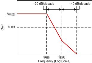
At any frequency lower than this ( 11.3 kHz), the power stage has a DC gain of 23 dB and at any higher frequency the power stage gain drops off at -40 dB per decade. The ESR zero is approximated in Equation 29.

Using two 100 µF, 2.5 mΩ ESR ceramic output capacitors, the calculated fESR of 636 kHz is greater than 1/5th the switching frequency, and therefore outside the scope of the error amplifier design. The gain of the power stage would change to –20 dB per decade above fESR. The straight line approximation the power stage gain is described in Figure 16.
The following compensation design procedure assumes fESR > fRES. For designs using large high-ESR bulk capacitors on the output where fESR < fRES. Type-II compensation can be used but is not described in this data sheet.
 Figure 16. Approximation of Power Stage Gain