JAJS448D March 2010 – October 2018 TPS54260
PRODUCTION DATA.
- 1 特長
- 2 アプリケーション
- 3 概要
- 4 改訂履歴
- 5 概要(続き)
- 6 Pin Configuration and Functions
- 7 Specifications
-
8 Detailed Description
- 8.1 Overview
- 8.2 Functional Block Diagram
- 8.3
Feature Description
- 8.3.1 Fixed Frequency PWM Control
- 8.3.2 Slope Compensation Output Current
- 8.3.3 Pulse-Skip Eco-Mode
- 8.3.4 Low-Dropout Operation and Bootstrap Voltage (BOOT)
- 8.3.5 Error Amplifier
- 8.3.6 Voltage Reference
- 8.3.7 Adjusting the Output Voltage
- 8.3.8 Enable and Adjusting Undervoltage Lockout
- 8.3.9 Slow-Start / Tracking Pin (SS/TR)
- 8.3.10 Overload Recovery Circuit
- 8.3.11 Sequencing
- 8.3.12 Constant Switching Frequency and Timing Resistor (RT/CLK Pin)
- 8.3.13 Overcurrent Protection and Frequency Shift
- 8.3.14 Selecting the Switching Frequency
- 8.3.15 How to Interface to RT/CLK Pin
- 8.3.16 Powergood (PWRGD Pin)
- 8.3.17 Overvoltage Transient Protection
- 8.3.18 Thermal Shutdown
- 8.3.19 Small Signal Model for Loop Response
- 8.3.20 Simple Small Signal Model for Peak Current Mode Control
- 8.3.21 Small Signal Model for Frequency Compensation
- 8.4 Device Functional Modes
-
9 Application and Implementation
- 9.1 Application Information
- 9.2
Typical Applications
- 9.2.1
3.3-V Output Application
- 9.2.1.1 Design Requirements
- 9.2.1.2
Detailed Design Procedure
- 9.2.1.2.1 Custom Design With WEBENCH® Tools
- 9.2.1.2.2 Selecting the Switching Frequency
- 9.2.1.2.3 Output Inductor Selection (LO)
- 9.2.1.2.4 Output Capacitor
- 9.2.1.2.5 Catch Diode
- 9.2.1.2.6 Input Capacitor
- 9.2.1.2.7 Slow-Start Capacitor
- 9.2.1.2.8 Bootstrap Capacitor Selection
- 9.2.1.2.9 Undervoltage Lock Out Set Point
- 9.2.1.2.10 Output Voltage and Feedback Resistors Selection
- 9.2.1.2.11 Compensation
- 9.2.1.2.12 Discontinuous Mode and Eco-Mode Boundary
- 9.2.1.2.13 Power Dissipation Estimate
- 9.2.1.3 Application Curves
- 9.2.2 Inverting Power Supply
- 9.2.3 Split-Rail Power Supply
- 9.2.4 12-V to 3.8-V GSM Power Supply
- 9.2.5 24-V to 4.2-V GSM Power Supply
- 9.2.1
3.3-V Output Application
- 10Power Supply Recommendations
- 11Layout
- 12デバイスおよびドキュメントのサポート
- 13メカニカル、パッケージ、および注文情報
パッケージ・オプション
メカニカル・データ(パッケージ|ピン)
サーマルパッド・メカニカル・データ
発注情報
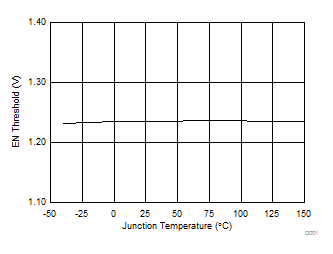
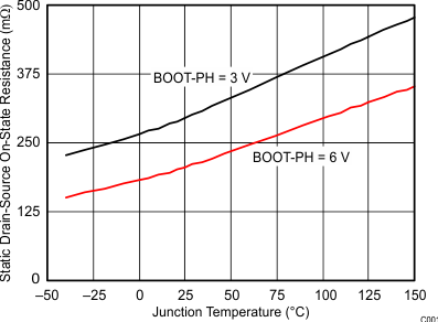
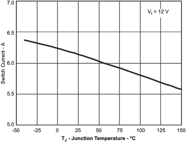
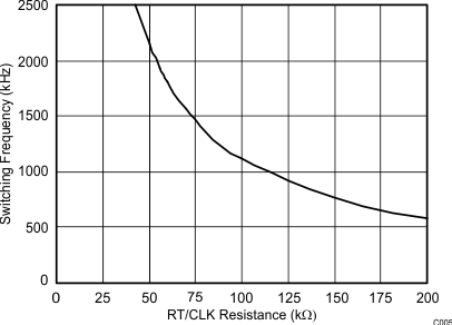
7.6 Typical Characteristics
| VI = 12 V |
| VI = 12 V | ||
| VI = 12 V | ||
| TJ = 25°C |
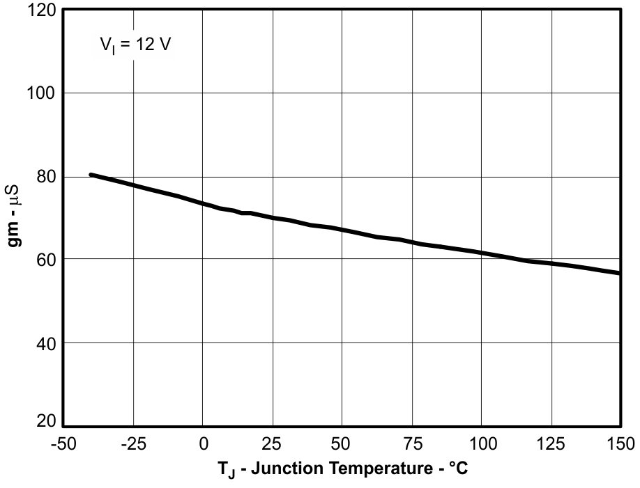 Figure 7. EA Transconductance During Slow-Start vs Junction Temperature
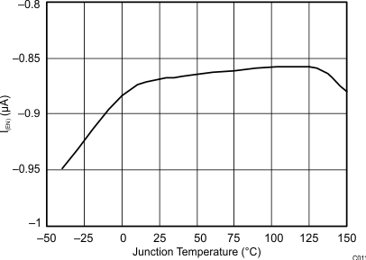
| VI = 12 V | ||
| VI(EN) = Theshold – 50 mV |
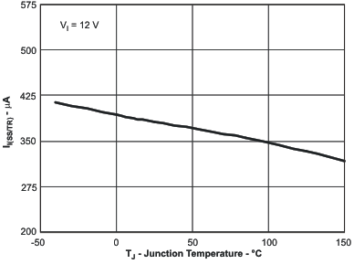
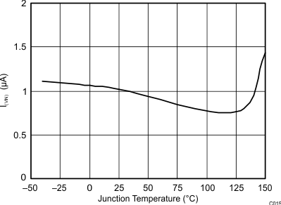
| VI = 12 V |
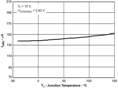 Figure 17. VIN Supply Current vs Junction Temperature
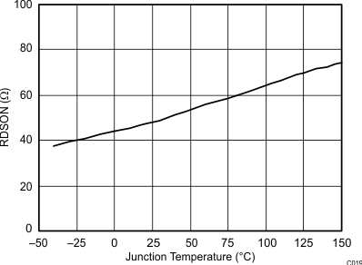
| VI = 12 V |
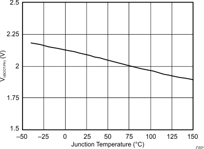 Figure 21. BOOT-PH UVLO vs Junction Temperature
 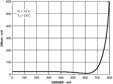 Figure 23. SS/TR to VSENSE Offset vs VSENSE
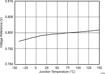
| VI = 12 V |
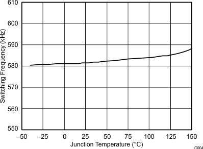
| VI = 12 V | ||
| RT = 200 kΩ | ||
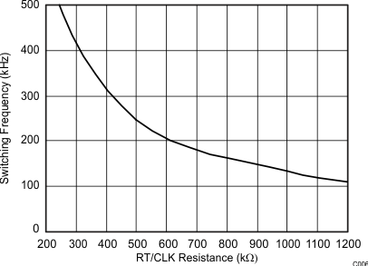
| VI = 12 V | ||
| TJ = 25°C |
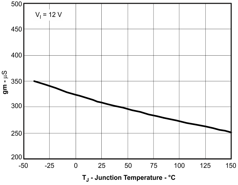 Figure 8. EA Transconductance vs Junction Temperature
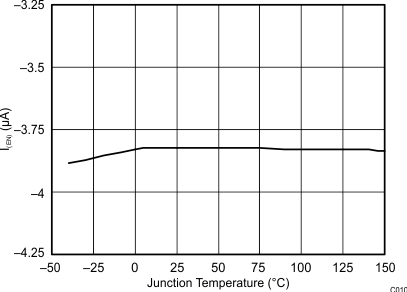
| VI = 12 V | ||
| VI(EN) = Theshold + 50 mV |
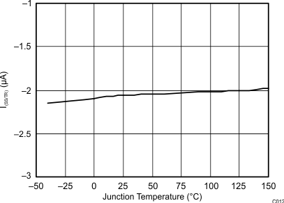
| VI = 12 V | ||
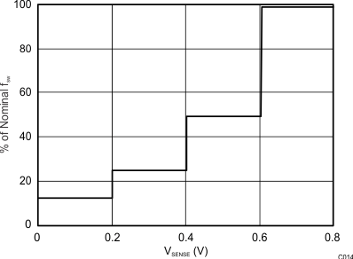
| VI = 12 V | ||
| TJ = 25°C |
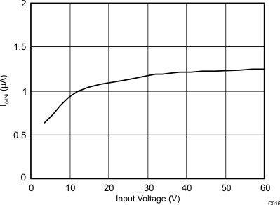
| TJ = 25°C |
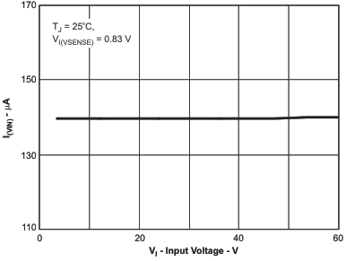 Figure 18. VIN Supply Current vs Input Voltage
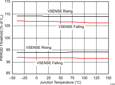
| VI = 12 V |
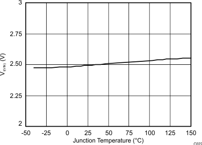 Figure 22. Input Voltage (UVLO) vs Junction Temperature
 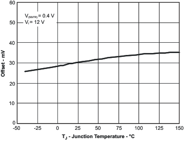 Figure 24. SS/TR to VSENSE Offset vs Temperature