JAJSDK1B May 2017 – March 2018 TPS543B20
PRODUCTION DATA.
- 1 特長
- 2 アプリケーション
- 3 概要
- 4 改訂履歴
- 5 Device Comparison Table
- 6 Pin Configuration and Functions
- 7 Specifications
-
8 Detailed Description
- 8.1 Overview
- 8.2 Functional Block Diagram
- 8.3 Feature Description
- 8.4
Device Functional Modes
- 8.4.1 Soft-Start Operation
- 8.4.2 Input and VDD Undervoltage Lockout (UVLO) Protection
- 8.4.3 Power Good and Enable
- 8.4.4 Voltage Reference
- 8.4.5 Prebiased Output Start-up
- 8.4.6 Internal Ramp Generator
- 8.4.7 Switching Frequency
- 8.4.8 Clock Sync Point Selection
- 8.4.9 Synchronization and Stackable Configuration
- 8.4.10 Dual-Phase Stackable Configurations
- 8.4.11 Operation Mode
- 8.4.12 API/BODY Brake
- 8.4.13 Sense and Overcurrent Protection
- 8.4.14 Output Overvoltage and Undervoltage Protection
- 8.4.15 Overtemperature Protection
- 8.4.16 RSP/RSN Remote Sense Function
- 8.4.17 Current Sharing
- 8.4.18 Loss of Synchronization
-
9 Application and Implementation
- 9.1 Application Information
- 9.2
Typical Application: TPS543B20 Stand-alone Device
- 9.2.1 Design Requirements
- 9.2.2 Detailed Design Procedure
- 9.2.3 Application Curves
- 9.3 System Example
- 10Power Supply Recommendations
- 11Layout
- 12デバイスおよびドキュメントのサポート
- 13メカニカル、パッケージ、および注文情報
パッケージ・オプション
メカニカル・データ(パッケージ|ピン)
- RVF|40
サーマルパッド・メカニカル・データ
- RVF|40
発注情報
8.4.7 Switching Frequency
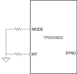
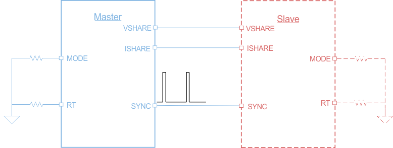
The converter supports analog frequency selections from 300 kHz to 2 MHz, for stand alone device and sync frequency from 300 kHz to 1 MHz for stackable configuration. The RT pin also sets clock sync point (SP) for the slave device.
Switching Frequency Configuration for Stand-alone and Master Device in Stackable Configuration
 Figure 14. Stand-alone: RT Pin Sets the Switching Frequency
  Figure 15. Stackable: Master (as Clock Master) RT Pin Sets Switching Frequency, and passes it to Slave
 Resistor RRT sets the continuous switching frequence selection by
Equation 1. 

where
- R is the resistor from RT pin to GND, in Ω
- ƒSW is the desired switching frequency, in Hz