JAJSDJ4D March 2016 – July 2017 TPS548D22
PRODUCTION DATA.
- 1 特長
- 2 アプリケーション
- 3 概要
- 4 改訂履歴
- 5 Description (continued)
- 6 Pin Configuration and Functions
- 7 Specifications
-
8 Detailed Description
- 8.1 Overview
- 8.2 Functional Block Diagram
- 8.3 Feature Description
- 8.4 Device Functional Modes
- 8.5 Programming
-
9 Application and Implementation
- 9.1 Application Information
- 9.2
Typical Applications
- 9.2.1 TPS548D22 1.5-V to 16-V Input, 1-V Output, 40-A Converter
- 9.2.2 Design Requirements
- 9.2.3
Design Procedure
- 9.2.3.1 Switching Frequency Selection
- 9.2.3.2 Inductor Selection
- 9.2.3.3 Output Capacitor Selection
- 9.2.3.4 Input Capacitor Selection
- 9.2.3.5 Bootstrap Capacitor Selection
- 9.2.3.6 BP Pin
- 9.2.3.7 R-C Snubber and VIN Pin High-Frequency Bypass
- 9.2.3.8 Optimize Reference Voltage (VSEL)
- 9.2.3.9 MODE Pin Selection
- 9.2.3.10 Overcurrent Limit Design.
- 9.2.4 Application Curves
- 10Power Supply Recommendations
- 11Layout
- 12デバイスおよびドキュメントのサポート
- 13メカニカル、パッケージ、および注文情報
- 14Package Option Addendum
8 Detailed Description
8.1 Overview
TPS548D22 device is a high-efficiency, single channel, FET-integrated, synchronous buck converter. It is suitable for point-of-load applications with 40 A or lower output current in storage, telecom and similar digital applications. The device features proprietary D-CAP3 mode control combined with adaptive on-time architecture. This combination is ideal for building modern high/low duty ratio, ultra-fast load step response DC-DC converters.
TPS548D22 device has integrated MOSFETs rated at 40-A TDC.
The converter input voltage range is from 1.5 V up to 16 V, and the VDD input voltage range is from 4.5 V to 22 V. The output voltage ranges from 0.6 V to 5.5 V.
Stable operation with all ceramic output capacitors is supported, since the D-CAP3 mode uses emulated current information to control the modulation. An advantage of this control scheme is that it does not require phase compensation network outside which makes it easy to use and also enables low external component count. The designer selects the switching frequency from 4 preset values via resistor settings by FSEL pin. Adaptive on-time control tracks the preset switching frequency over a wide range of input and output voltage while increasing switching frequency as needed during load step transient.
8.2 Functional Block Diagram
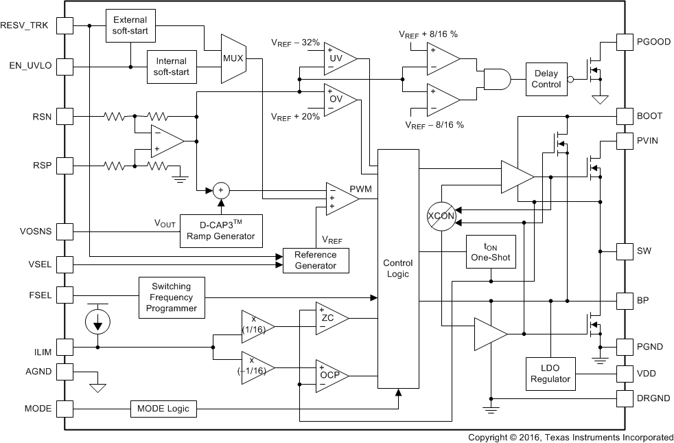
8.3 Feature Description
8.3.1 40-A FET
The TPS548D22 device is a high-performance, integrated FET converter supporting current rating up to 40 A thermally. It integrates two N-channel NexFET™ power MOSFETs, enabling high power density and small PCB layout area. The drain-to-source breakdown voltage for these FETs is 25 V DC and 27 V transient for 10 ns. Avalanche breakdown occurs if the absolute maximum voltage rating exceeds 27 V. In order to limit the switch node ringing of the device, it is recommended to add a R-C snubber from the SW node to the PGND pins. Refer to the Layout Guidelines section for the detailed recommendations.
8.3.2 On-Resistance
The typical on-resistance (RDS(on)) for the high-side MOSFET is 2.9 mΩ and typical on-resistance for the low-side MOSFET is 1.2 mΩ with a nominal gate voltage (VGS) of 5 V.
8.3.3 Package Size, Efficiency and Thermal Performance
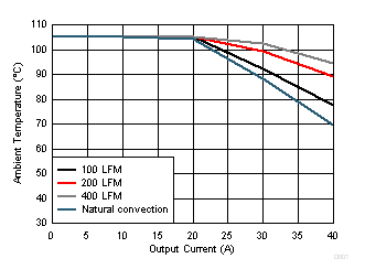
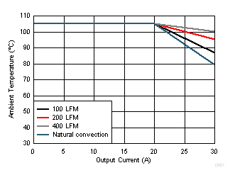
The TPS548D22 device is available in a 5 mm x 7 mm, QFN package with 40 power and I/O pins. It employs TI proprietary MCM packaging technology with thermal pad. With a properly designed system layout, applications achieve optimized safe operating area (SOA) performance. The curves shown in Figure 12 and Figure 13 are based on the orderable evaluation module design. (See SLUUBE4 to order the EVM)
8.3.4 Soft-Start Operation
In the TPS548D22 device the soft-start time controls the inrush current required to charge the output capacitor bank during startup. The device offers selectable soft-start options of 1 ms, 2 ms, 4 ms and 8 ms. When the device is enabled (either by EN or VDD UVLO), the reference voltage ramps from 0 V to the final level defined by VSEL pin strap configuration, in a given soft-start time. The TPS548D22 device supports several soft-start times between 1msec and 8msec selected by MODE pin configuration. Refer to MODE definition table for details.
8.3.5 VDD Supply Undervoltage Lockout (UVLO) Protection
The TPS548D22 device provides fixed VDD undervoltage lockout threshold and hysteresis. The typical VDD turn-on threshold is 4.25 V and hysteresis is 0.2 V. The VDD UVLO can be used in conjunction with the EN_UVLO signal to provide proper power sequence to the converter design. UVLO is a non-latched protection.
8.3.6 EN_UVLO Pin Functionality
The EN_UVLO pin drives an input buffer with accurate threshold and can be used to program the exact required turn-on and turn-off thresholds for switcher enable, VDD UVLO or VIN UVLO (if VIN and VDD are tied together). If desired, an external resistor divider can be used to set and program the turn-on threshold for VDD or VIN UVLO.
Figure 14 shows how to program the input voltage UVLO using the EN_UVLO pin.
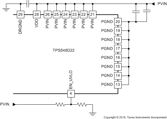 Figure 14. Programming the UVLO Voltage
8.3.7 Fault Protections
This section describes positive and negative overcurrent limits, overvoltage protections, out-of-bounds limits, undervoltage protections and over temperature protections.
8.3.7.1 Current Limit (ILIM) Functionality
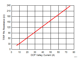 Figure 15. Current Limit Resistance vs OCP Valley Overcurrent Limit
The ILIM pin sets the OCP level. Connect the ILIM pin to GND through the voltage setting resistor, RILIM. In order to provide both good accuracy and cost effective solution, TPS548D22 device supports temperature compensated internal MOSFET RDS(on) sensing.
Also, the TPS548D22 device performs both positive and negative inductor current limiting with the same magnitudes. The positive current limit normally protects the inductor from saturation that causes damage to the high-side FET and low-side FET. The negative current limit protects the low-side FET during OVP discharge.
The voltage between GND pin and SW pin during the OFF time monitors the inductor current. The current limit has 3000 ppm/°C temperature slope to compensate the temperature dependency of the on-resistance (RDS(on)). The GND pin is used as the positive current sensing node.
TPS548D22 device uses cycle-by-cycle over-current limiting control. The inductor current is monitored during the OFF state and the controller maintains the OFF state during the period that the inductor current is larger than the overcurrent ILIM level. VILIM sets the valley level of the inductor current.
8.3.7.2 VDD Undervoltage Lockout (UVLO)
The TPS548D22 device has an UVLO protection function for the VDD supply input. The on-threshold voltage is 4.25 V with 200 mV of hysteresis. During a UVLO condition, the device is disabled regardless of the EN_UVLO pin voltage. The supply voltage (VVDD) must be above the on-threshold to begin the pin strap detection.
8.3.7.3 Overvoltage Protection (OVP) and Undervoltage Protection (UVP)
The device monitors a feedback voltage to detect overvoltage and undervoltage. When the feedback voltage becomes lower than 68% of the target voltage, the UVP comparator output goes high and an internal UVP delay counter begins counting. After 1 ms, the device latches OFF both high-side and low-side MOSFETs drivers. The UVP function enables after soft-start is complete.
When the feedback voltage becomes higher than 120% of the target voltage, the OVP comparator output goes high and the circuit latches OFF the high-side MOSFET driver and turns on the low-side MOSFET until reaching a negative current limit. Upon reaching the negative current limit, the low-side FET is turned off and the high-side FET is turned on again for a minimum on-time. The TPS548D22 device operates in this cycle until the output voltage is pulled down under the UVP threshold voltage for 1 ms. After the 1-ms UVP delay time, the high-side FET is latched off and low-side FET is latched on. The fault is cleared with a reset of VDD or by retoggling the EN pin.
Table 1. Overvoltage Protection Details
| REFERENCE VOLTAGE (VREF) |
SOFT-START RAMP | STARTUP OVP THRESHOLD | OPERATING OVP THRESHOLD | OVP DELAY 100 mV OD (µs) |
OVP RESET |
|---|---|---|---|---|---|
| Internal | Internal | 1.2 × Internal VREF | 1.2 × Internal VREF | 1 | UVP |
8.3.7.4 Out-of-Bounds Operation
The device has an out-of-bounds (OOB) overvoltage protection that protects the output load at a much lower overvoltage threshold of 8% above the target voltage. OOB protection does not trigger an overvoltage fault, so the device is not latched off after an OOB event. OOB protection operates as an early no-fault overvoltage-protection mechanism. During the OOB operation, the controller operates in forced PWM mode only by turning on the low-side FET. Turning on the low-side FET beyond the zero inductor current quickly discharges the output capacitor thus causing the output voltage to fall quickly toward the setpoint. During the operation, the cycle-by-cycle negative current limit is also activated to ensure the safe operation of the internal FETs.
8.3.7.5 Overtemperature Protection
TPS548D22 device has overtemperature protection (OTP) by monitoring the die temperature. If the temperature exceeds the threshold value (default value 165°C), TPS548D22 device is shut off. When the temperature falls about 25°C below the threshold value, the device turns on again. The OTP is a non-latch protection.
8.4 Device Functional Modes
8.4.1 DCAP3 Control Topology
The TPS548D22 employs an artificial ramp generator that stabilizes the loop. The ramp amplitude is automatically adjusted as a function of selected switching frequency (fSW) The ramp amplitude is a function of duty cycle (VOUT-to-VIN ratio). Consequently, two additional pin-strap bits (FSEL[2:1]) are provided for fine tuning the internal ramp amplitude. The device uses an improved DCAP3 control loop architecture that incorporates a steady-state error integrator. The slow integrator improves the output voltage DC accuracy greatly and presents minimal impact to small signal transient response. To further enhance the small signal stability of the control loop, the device uses a modified ramp generator that supports a wider range of output LC stage.
8.4.2 DCAP Control Topology
For advanced users of this device, the internal DCAP3 ramp can be disabled using the MODE[4] pin strap bit. This situation requires an external RCC network to ensure control loop stability. Place this RCC network across the output inductor. Use a range between 10 mV and 15 mV of injected RSP pin ripple. If no feedback resistor divider network is used, insert a 10-kΩ resistor between the VOUT pin and the RSP pin.
8.5 Programming
8.5.1 Programmable Pin-Strap Settings
FSEL, VSEL, and MODE. Description: a 1% or better 100-kΩ resistor is needed from BP to each of the three pins. The bottom resistor from each pin to ground (see Table 2 ) in conjunction with the top resistor defines each pin strap selection. The pin detection checks for external resistor divider ratio during initial power up (VDD is brought down below approximately 3 V) when BP LDO output is at approximately 2.9 V.
8.5.1.1 Frequency Selection (FSEL) Pin
The TPS548D22 device allows users to select the switching frequency, light load and internal ramp amplitude by using FSEL pin. Table 2 lists the divider resistor values for the selection. The 1% tolerance resistors with typical temperature coefficient of ±100ppm/°C are recommended. Higher performance resistors can be used if tighter noise margin is required for more reliable frequency selection detection.
FSEL pin strap configuration programs the switching frequency, internal ramp compensation and light load conduction mode.
Table 2. FSEL Pin Strap Configurations
| FSEL[4] | FSEL[3] | FSEL[2] | FSEL[1] | FSEL[0] | RFSEL (kΩ) (1) |
|---|---|---|---|---|---|
| FSEL[1:0] | RCSP_FSEL[1:0] | CM | |||
| 11: 1.05 MHz | 11: R × 3 | 1: FCCM | Open | ||
| 0: SKIP | 187 | ||||
| 10: R × 2 | 1: FCCM | 165 | |||
| 0: SKIP | 147 | ||||
| 01: R × 1 | 1: FCCM | 133 | |||
| 0: SKIP | 121 | ||||
| 00: R/2 | 1: FCCM | 110 | |||
| 0: SKIP | 100 | ||||
| 10: 875 kHz | 11: R × 3 | 1: FCCM | 90.9 | ||
| 0: SKIP | 82.5 | ||||
| 10: R × 2 | 1: FCCM | 75 | |||
| 0: SKIP | 68.1 | ||||
| 01: R × 1 | 1: FCCM | 60.4 | |||
| 0: SKIP | 53.6 | ||||
| 00: R/2 | 1: FCCM | 47.5 | |||
| 0: SKIP | 42.2 | ||||
| 01: 650 kHz | 11: R × 3 | 1: FCCM | 37.4 | ||
| 0: SKIP | 33.2 | ||||
| 10: R × 2 | 1: FCCM | 29.4 | |||
| 0: SKIP | 25.5 | ||||
| 01: R × 1 | 1: FCCM | 22.1 | |||
| 0: SKIP | 19.1 | ||||
| 00: R/2 | 1: FCCM | 16.5 | |||
| 0: SKIP | 14.3 | ||||
| 00: 425 kHz | 11: R × 3 | 1: FCCM | 12.1 | ||
| 0: SKIP | 10 | ||||
| 10: R × 2 | 1: FCCM | 7.87 | |||
| 0: SKIP | 6.19 | ||||
| 01: R × 1 | 1: FCCM | 4.64 | |||
| 0: SKIP | 3.16 | ||||
| 00: R/2 | 1: FCCM | 1.78 | |||
| 0: SKIP | 0 | ||||
8.5.1.2 VSEL Pin
VSEL pin strap configuration is used to program initial boot voltage value, hiccup mode, and latch-off mode. The initial boot voltage is used to program the main loop voltage reference point. VSEL voltage settings provide TI designated discrete internal reference voltages. Table 3 lists internal reference voltage selections.
Table 3. Internal Reference Voltage Selections
| VSEL[4] | VSEL[3] | VSEL[2] | VSEL[1] | VSEL[0] | RVSEL (kΩ) (1) |
|---|---|---|---|---|---|
| 1111: 0.975 V | 1: Latch-Off | Open | |||
| 0: Hiccup | 187 | ||||
| 1110: 1.1992 V | 1: Latch-Off | 165 | |||
| 0: Hiccup | 147 | ||||
| 1101: 1.1504 V | 1: Latch-Off | 133 | |||
| 0: Hiccup | 121 | ||||
| 1100: 1.0996 V | 1: Latch-Off | 110 | |||
| 0: Hiccup | 100 | ||||
| 1011: 1.0508 V | 1: Latch-Off | 90.9 | |||
| 0: Hiccup | 82.5 | ||||
| 1010: 1.0000 V | 1: Latch-Off | 75 | |||
| 0: Hiccup | 68.1 | ||||
| 1001: 0.9492 V | 1: Latch-Off | 60.4 | |||
| 0: Hiccup | 53.6 | ||||
| 1000: 0.9023 V | 1: Latch-Off | 47.5 | |||
| 0: Hiccup | 42.2 | ||||
| 0111: 0.9004 V | 1: Latch-Off | 37.4 | |||
| 0: Hiccup | 33.2 | ||||
| 0110: 0.8496 V | 1: Latch-Off | 29.4 | |||
| 0: Hiccup | 25.5 | ||||
| 0101: 0.8008 V | 1: Latch-Off | 22.1 | |||
| 0: Hiccup | 19.1 | ||||
| 0100: 0.7500 V | 1: Latch-Off | 16.5 | |||
| 0: Hiccup | 14.3 | ||||
| 0011: 0.6992 V | 1: Latch-Off | 12.1 | |||
| 0: Hiccup | 10 | ||||
| 0010: 0.6504 V | 1: Latch-Off | 7.87 | |||
| 0: Hiccup | 6.19 | ||||
| 0001: 0.5996 V | 1: Latch-Off | 4.64 | |||
| 0: Hiccup | 3.16 | ||||
| 0000: 0.975 V | 1: Latch-Off | 1.78 | |||
| 0: Hiccup | 0 | ||||
8.5.1.3 DCAP3 Control and Mode Selection
The MODE pinstrap configuration programs the control topology and internal soft-start timing selections. The TPS548D22 device supports both DCAP3 and DCAP operation
MODE[4] selection bit is used to set the control topology. If MODE[4] bit is 0, it selects DCAP operation. If MODE[4] bit is 1, it selects DCAP3 operation.
MODE[1] and MODE[0] selection bits are used to set the internal soft-start timing.
Table 4. Allowable MODE Pin Selections
| MODE[4] | MODE[3] | MODE[2] | MODE[1] | MODE[0] | RMODE (kΩ) (1) |
|---|---|---|---|---|---|
| 1: DCAP3 | 0: Internal Reference | 0: Internal SS | 11: 8 ms(1) | 60.4 | |
| 10: 4 ms(1) | 53.6 | ||||
| 01: 2 ms | 47.5 | ||||
| 00: 1 ms | 42.2 | ||||
| 0: DCAP | 0: Internal Reference | 0: Internal SS | 11: 8 ms(1) | 4.64 | |
| 10: 4 ms(1) | 3.16 | ||||
| 01: 2 ms | 1.78 | ||||
| 00: 1 ms | 0 | ||||
8.5.1.3.1 Application Workaround to Support 4-ms and 8-ms SS Settings
In order to properly design for 4-ms and 8-ms SS settings, additional application consideration is needed. The recommended application workaround to support the 4-ms and 8-ms soft-start settings is to ensure sufficient time delay between the VDD and EN_UVLO signals. The minimum delay between the rising maximum VDD_UVLO level and the minimum turnon threshold of EN_UVLO is at least TDELAY_MIN.
where
- K = 9 ms/V for SS setting of 4 ms
- K = 18 ms/V for SS setting of 8 ms
- VREF is the internal reference voltage programmed by VSEL pin strap
For example, if SS setting is 4 ms and VREF = 1 V, program the minimum delay at least 9 ms; if SS setting is 8 ms, the minimum delay should be programmed at least 18 ms. See Figure 16 and Figure 17 for detailed timing requirement.
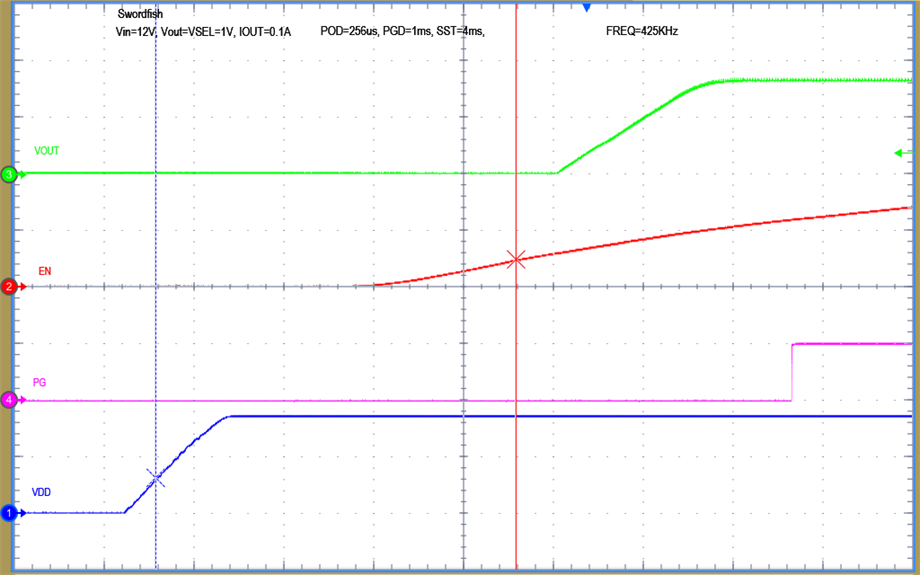 Figure 16. Proper Sequencing of VDD and EN_UVLO to Support the use of 4-ms SS Setting
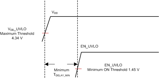 Figure 17. Minimum Delay Between VDD and EN_UVLO to Support the use of 4-ms and 8-ms SS settings
The workaround/consideration described previously is not required for SS settings of 1 ms and 2 ms.
8.5.2 Programmable Analog Configurations
8.5.2.1 RSP/RSN Remote Sensing Functionality
RSP and RSN pins are used for remote sensing purpose. In the case where feedback resistors are required for output voltage programming, the RSP pin must be connected to the mid-point of the resistor divider, and the RSN pin must always be connected to the load return. In the case where feedback resistors are not required, such as when the VSEL programs the output voltage setpoint, the RSP pin must be connected to the positive sensing point of the load, and the RSN pin should always be connected to the load return.
RSP and RSN pins are extremely high-impedance input terminals of the true differential remote sense amplifier. The feedback resistor divider should use resistor values much less than 100 kΩ.
8.5.2.1.1 Output Differential Remote Sensing Amplifier
The examples in this section show simplified remote sensing circuitry where each example uses an internal reference of 1 V. Figure 18 shows remote sensing without feedback resistors, with an output voltage set point of 1 V. Figure 19 shows remote sensing using feedback resistors, with an output voltage set point of 5 V.
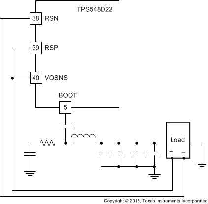 Figure 18. Remote Sensing Without Feedback Resistors
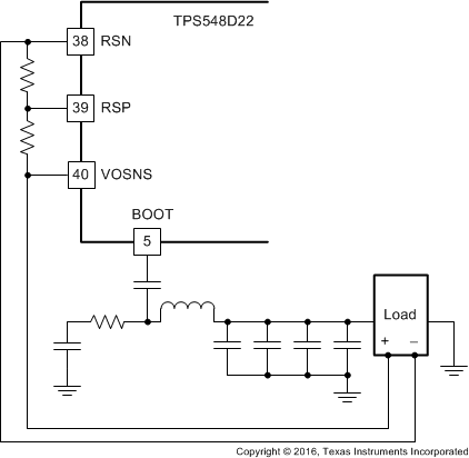 Figure 19. Remote Sensing With Feedback Resistors
8.5.2.2 Power Good (PGOOD Pin) Functionality
The TPS548D22 device has power-good output that registers high when switcher output is within the target. The power-good function is activated after soft-start has finished. When the soft-start ramp reaches 300 mV above the internal reference voltage, SSend signal goes high to enable the PGOOD detection function. If the output voltage becomes within ±8% of the target value, internal comparators detect power-good state and the power good signal becomes high after an 8-ms programmable delay. If the output voltage goes outside of ±16% of the target value, the power good signal becomes low after two microsecond (2-µs) internal delay. The open-drain power-good output must be pulled up externally. The internal N-channel MOSFET does not pull down until the VDD supply is above 1.2 V.
