JAJSCL3C October 2016 – August 2023 TPS568215
PRODUCTION DATA
- 1
- 1 特長
- 2 アプリケーション
- 3 概要
- 4 Revision History
- 5 Pin Configuration and Functions
- 6 Specifications
-
7 Detailed Description
- 7.1 Overview
- 7.2 Functional Block Diagram
- 7.3
Feature Description
- 7.3.1 PWM Operation and D-CAP3 Control Mode
- 7.3.2 Eco-mode Control
- 7.3.3 4.7 V LDO and External Bias
- 7.3.4 MODE Selection
- 7.3.5 Soft Start and Pre-biased Soft Start
- 7.3.6 Enable and Adjustable UVLO
- 7.3.7 Power Good
- 7.3.8 Overcurrent Protection and Undervoltage Protection
- 7.3.9 Out-of-Bounds Operation
- 7.3.10 UVLO Protection
- 7.3.11 Thermal Shutdown
- 7.3.12 Output Voltage Discharge
- 7.4 Device Functional Modes
- 8 Application and Implementation
- 9 Device and Documentation Support
- 10Mechanical, Packaging, and Orderable Information
8.2.2.1.3 Inductor Selection
The inductor ripple current is filtered by the output capacitor. A higher inductor ripple current means the output capacitor must have a ripple current rating higher than the inductor ripple current. See Table 8-2 for recommended inductor values.
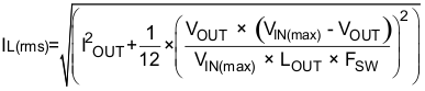
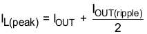
The RMS and peak currents through the inductor can be calculated using Equation 7 and Equation 8. It is important that the inductor is rated to handle these currents.
During transient/short circuit conditions the inductor current can increase up to the current limit of the device so it is safe to choose an inductor with a saturation current higher than the peak current under current limit condition.