JAJSCL3C October 2016 – August 2023 TPS568215
PRODUCTION DATA
- 1
- 1 特長
- 2 アプリケーション
- 3 概要
- 4 Revision History
- 5 Pin Configuration and Functions
- 6 Specifications
-
7 Detailed Description
- 7.1 Overview
- 7.2 Functional Block Diagram
- 7.3
Feature Description
- 7.3.1 PWM Operation and D-CAP3 Control Mode
- 7.3.2 Eco-mode Control
- 7.3.3 4.7 V LDO and External Bias
- 7.3.4 MODE Selection
- 7.3.5 Soft Start and Pre-biased Soft Start
- 7.3.6 Enable and Adjustable UVLO
- 7.3.7 Power Good
- 7.3.8 Overcurrent Protection and Undervoltage Protection
- 7.3.9 Out-of-Bounds Operation
- 7.3.10 UVLO Protection
- 7.3.11 Thermal Shutdown
- 7.3.12 Output Voltage Discharge
- 7.4 Device Functional Modes
- 8 Application and Implementation
- 9 Device and Documentation Support
- 10Mechanical, Packaging, and Orderable Information
7.3.2 Eco-mode Control
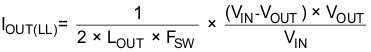
The TPS568215 is designed with Eco-mode™ control to increase efficiency at light loads. This option can be chosen using the MODE pin as shown in table 3. As the output current decreases from heavy load condition, the inductor current is also reduced. If the output current is reduced enough, the valley of the inductor current reaches the zero level, which is the boundary between continuous conduction and discontinuous conduction modes. The low-side MOSFET is turned off when a zero inductor current is detected. As the load current further decreases the converter runs into discontinuous conduction mode. The on-time is kept approximately the same as it is in continuous conduction mode. The off-time increases as it takes more time to discharge the output with a smaller load current. The light load current where the transition to Eco-mode™ operation happens ( IOUT(LL) ) can be calculated from Equation 2.
After identifying the application requirements, design the output inductance so that the inductor peak-to-peak ripple current is approximately between 20% and 30% of the ICC(ma×) (peak current in the application). it is also important to size the inductor properly so that the valley current doesn't hit the negative low side current limit.