JAJSII5A January   2020  – March 2020 TPS59603-Q1

PRODUCTION DATA.  

  1. 特長
  2. アプリケーション
  3. 概要
    1.     Device Images
      1.      アプリケーション概略図
  4. 改訂履歴
  5. Pin Configuration and Functions
    1.     Pin Functions
  6. Specifications
    1. 6.1 Absolute Maximum Ratings
    2. 6.2 ESD Ratings
    3. 6.3 Recommended Operating Conditions
    4. 6.4 Thermal Information
    5. 6.5 Electrical Characteristics
    6. 6.6 Typical Characteristics
  7. Detailed Description
    1. 7.1 Overview
    2. 7.2 Functional Block Diagram
    3. 7.3 Feature Description
      1. 7.3.1 UVLO Protection
      2. 7.3.2 PWM Pin
      3. 7.3.3 SKIP Pin
        1. 7.3.3.1 Zero Crossing (ZX) Operation
      4. 7.3.4 Adaptive Dead-Time Control and Shoot-Through Protection
      5. 7.3.5 Integrated Boost-Switch
    4. 7.4 Device Functional Modes
  8. Power Supply Recommendations
  9. Layout
    1. 9.1 Layout Guidelines
    2. 9.2 Layout Recommendation
  10. 10デバイスおよびドキュメントのサポート
    1. 10.1 デバイス・サポート
      1. 10.1.1 開発サポート
    2. 10.2 ドキュメントのサポート
      1. 10.2.1 関連資料
    3. 10.3 コミュニティ・リソース
    4. 10.4 商標
    5. 10.5 静電気放電に関する注意事項
    6. 10.6 Glossary
  11. 11メカニカル、パッケージ、および注文情報

パッケージ・オプション

メカニカル・データ(パッケージ|ピン)
サーマルパッド・メカニカル・データ
発注情報

Adaptive Dead-Time Control and Shoot-Through Protection

The driver utilizes an anti-shoot-through and adaptive dead-time control to minimize low-side body diode conduction time and maintain high efficiency. When the PWM input voltage becomes high, the low-side MOSFET gate voltage begins to fall after a propagation delay. At the same time, DRVL voltage is sensed, and high-side driving voltage starts to increase after DRVL voltage is lower than a proper threshold.
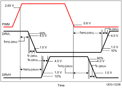
TPS59603-Q1 v12226_lusba6.gifFigure 15. Rise and Fall Timing and Propagation Delay Definitions

Typical operation manages to near zero the dead-time between the low-side gate turn-off to high-side gate voltage turn-on, and high-side gate turn-off to low-side gate turn-on, in order to avoid simultaneous conduction of both MOSFETs, as well as to reduce body diode conduction and recovery losses. This operation also reduces ringing on the leading edge of the SW waveform.
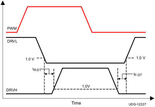
TPS59603-Q1 v12227_lusba6.gifFigure 16. Dead-Time Definitions